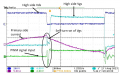
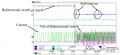
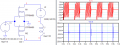
full-bridge CLLC, high side Mosfet Vgs weird

Janis59

Joined Aug 21, 2017
1,893
Aaaa, ow. That is old known effect I am suffering sometimes even now. The upper `on` voltage form is perfect all cases, but when upper is `off`, the time moments when lower shoulders are making `on` and `off` transients, are observed unpleasantly high peaks what are creating nanosecond scale throughput currents in upper, thus the unneeded heating and overstress. Strangest, the Spice modell shows it MUST be there as the effect inherrently. Then I started to meditate about Miller killer. Sure the effect is happening because of C(gs). The simplest solution is pass the better combination of gate driver and mosfet/igbt itself. More harder way is to play with Rg value or shift it to inductive, apply diodes etc etc. Third is set the such power keys what are sure not reacting to those 3-4 Volt delta needles. And last but no least - dance around the Tote Pole, however I bet the Vsd transient beating have very minor effect about the remedy if any at all.
 

Thread Starter

kinghero1989

Joined Aug 8, 2023
24
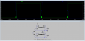
These spikes, exactly at start of deadtime,
should be negative, not positive:

View attachment 300106
ADDED:
1. In your case it may be capacitive coupling between 15 V power supplies.
2. Check signal waveform on driver input
Do you think this is because of the layout problem? I also do simulations but can't see the phenomenal as the practical circuit
 

Thread Starter

kinghero1989

Joined Aug 8, 2023
24
Aaaa, ow. That is old known effect I am suffering sometimes even now. The upper `on` voltage form is perfect all cases, but when upper is `off`, the time moments when lower shoulders are making `on` and `off` transients, are observed unpleasantly high peaks what are creating nanosecond scale throughput currents in upper, thus the unneeded heating and overstress. Strangest, the Spice modell shows it MUST be there as the effect inherrently. Then I started to meditate about Miller killer. Sure the effect is happening because of C(gs). The simplest solution is pass the better combination of gate driver and mosfet/igbt itself. More harder way is to play with Rg value or shift it to inductive, apply diodes etc etc. Third is set the such power keys what are sure not reacting to those 3-4 Volt delta needles. And last but no least - dance around the Tote Pole, however I bet the Vsd transient beating have very minor effect about the remedy if any at all.
I suspect the layout problem, do you think so?
 

Danko

Joined Nov 22, 2017
2,196
2. Check signal waveform on driver input
I check the input of the gate driver. It seems the reason for the spike, do you have any idea for solving the problem?
Check current from ground of capacitor 400V to ground of H-bridge.
If extra current pulses are not exist, then positive spikes on
gates are artefacts, simple signal, received by oscilloscope
and by probe cable shield, which is working like antenna.
ADDED:
It should be something like this, w/o spikes on it:
1691857816005.png
 
Last edited:

Thread Starter

kinghero1989

Joined Aug 8, 2023
24
Check current from ground of capacitor 400V to ground of H-bridge.
If extra current pulses are not exist, then positive spikes on
gates are artefacts, simple signal, received by oscilloscope
and by probe cable shield, which is working like antenna.
ADDED:
It should be something like this, w/o spikes on it:
View attachment 300343
Do you guys think MOSFETs' rise and fall time is too fast? Should I reduce it to reduce the spike?
 

Attachments

Thread Starter

kinghero1989

Joined Aug 8, 2023
24
Thank you for your informaion
Vgs of both sides look just perfect.
If you want to see more real picture of waveform,
try pseudo-differential measuring of them.
https://www.tek.com/en/support/faqs/how-can-i-make-differential-measurement-passive-probes
Increasing rise and fall times will increase heating of MOSFETs.
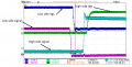
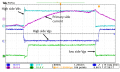
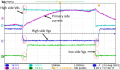
This is the waveform at 2kW. The waveform looks similar to your simulation but has a bit small spike. Please have a look at it. Do you think it's ok? Thank you.
 

Attachments

Danko

Joined Nov 22, 2017
2,196
This is the waveform at 2kW. The waveform looks similar to your simulation but has a bit small spike. Please have a look at it. Do you think it's ok? Thank you.
Primary side current defined by transformer quality and IV characteristic of load.
Gate voltages seems good.
Transition processes of transistors switching may affect measurement system.
So you can double check signal on low side gate, assuming that signal on high side gate is identical.
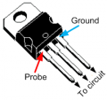
Measurement should be performed by this way:
1692018538932.png

1692015376618.png
 

SiCEngineer

Joined May 22, 2019
444
I am working on full-bridge CLLC, and the waveform I got is quite weird. Is there anyone who has such kind of experience?
Have you considered using a negative gate drive voltage for turning the device off? Silicon carbide FETs tend to implement something like +15V-4V in their gate drive to avoid this type of problem.
 

Thread Starter

kinghero1989

Joined Aug 8, 2023
24
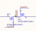
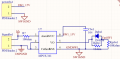
Hi guys, I am doing the bidirectional power switch. I am wondering if could I use the same gate driver and the same gate resistor for both N-channel Mosfet as in the picture below, or do I need to separate them?
 

Attachments

Danko

Joined Nov 22, 2017
2,196
Is your load inductive?
1692640188795.png
ADDED:
Only full bridge is resistive to HV spikes.
Bidirectional power switch does not.
Even first transition from ON to OFF may destroy FETs.
EDIT:
Simulation is reconstructed.
 

Attachments

Last edited:
Top