 Facebook
 Google
 GitHub
 Linkedin
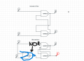
Hi.A simple SR latch has the issue that if both set and reset are 1 the state of Q becomes undefined since it relies on which side wins the battle of trying to set Q = 0 or 1.
However if instead of 2 pins S and R independent of each other, the NOR or NAND gate which was connected to either Q or Q' input which is not part of the feedback path(since Q is fed into the input for Q' and vice versa) was NOR of SR so instead of S and R pins we had S or R pin and a NOR(S,R) wouldnt that force 2 memory conditions(remove the problematic case of S=1,R=1)?
However if instead of 2 pins S and R independent of each other, the NOR or NAND gate which was connected to either Q or Q' input which is not part of the feedback path(since Q is fed into the input for Q' and vice versa) was NOR of SR so instead of S and R pins we had S or R pin and a NOR(S,R) wouldnt that force 2 memory conditions(remove the problematic case of S=1,R=1)?
Attachments
-
 134.1 KB Views: 26
Last edited:


