Facebook
 Google
 GitHub
 Linkedin
Hello,
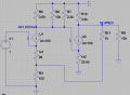
I've been looking at feedback amplifiers such as the one below and the overall gain of the amplifier is equal to R11/R3. Knowing this is great but I'm trying to understand the gain of each of the two stages. Figuring this out is easy without the feedback path, you calculate Zin, Zbase, gain of each stage, etc. But with feedback path its not so easy, so how should I go about calculating the gain of each stage?
Thanks
Attachments
-
 11.3 KB Views: 79