 Facebook
 Google
 GitHub
 Linkedin
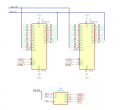
Looking at this, is it safe to assume that the two EPROMs are NOT consecutive in memory?
If one were to replace these two 2516s with a single 2764, the data loaded into the 2764 would be image M-0 / blank / image M-1 / blank, correct?
If one were to replace these two 2516s with a single 2764, the data loaded into the 2764 would be image M-0 / blank / image M-1 / blank, correct?
Attachments
-
 39.1 KB Views: 18


