EDM - Electrical discharge machine

LesJones

Joined Jan 8, 2017
4,190
Hi SB,
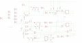
There's nothing in post#60 that needs commenting on. I started to draw out a version of your schematic (From post #16) that does not use the D and clock inputs on the flipflops. (I think this will require less components but I won't know until is finish it.) I noticed a few errors. The first one is that the start button sets the discharge flipflop aswell as the charge flipflop. I dont think this should happen. Diode D2 in block 2 is the wrong way round. You will also need to add a power on reset circuit so the flipflops are both in the reset state to start with. I should have noticed the drop down box when I highlighted the text I wanted to copy. I will try it next time I need to quote any of your post.
Edit. I have just noticed another problem. The D input on the discharge flipflop is not connected to anything. (Unused inputs on CMOS logic should not be left floating. it should be connected to ground or the positive supply rail.) I thought at first connecting it to the output of the upper comparator in block 5 would solve the problem but it would be changing state at almost the same time as the clock pulse was going from low to high so the flip flop may not get set. It may be possible to delay the clock pulse sllightly with a capacitor and resistor but this in not good practice.

Les.
 
Last edited:

Thread Starter

shortbus

Joined Sep 30, 2009
10,045
Hi Les. I am going to start redrawing, and can't wait to see what you come up with. Things have been hectic here lately so may take a day or so.

I started to draw out a version of your schematic (From post #16) that does not use the D and clock inputs on the flipflops.
I used the "D" and clock to make the flipflops into toggle type FF. The set and rest aren't edge triggered are they? Without an edge trigger I can't see how it will work, but then what do I know?

I noticed a few errors. The first one is that the start button sets the discharge flipflop aswell as the charge flipflop. I dont think this should happen. Diode D2 in block 2 is the wrong way round. You will also need to add a power on reset circuit so the flipflops are both in the reset state to start with.
The start really is doing two things and there is a reason I did it the way it is, by my understanding of things. The first part Block #1, sets the notQ on the FF's to make the circuit ready. This the turns on Q2 and Q4, which are necessary to charge both bootstrap caps so when the circuit starts Q1 and Q3 will work. Without the boot caps charged the circuit won't run by it's self.

Then when Block #1 times out, and Block #2 sees the falling edge of that signal, the charge FF will change to Q and the cap bank starts to charge starting the whole circuit into running step by step until it gets shut off.

The D input on the discharge flipflop is not connected to anything. (Unused inputs on CMOS logic should not be left floating.
That could be very possible. I had to move things around when I was drawing it and could have missed the connection. I do know about unused inputs so it wasn't intentional, but accidental.
 

LesJones

Joined Jan 8, 2017
4,190
Hi SB,

I used the "D" and clock to make the flipflops into toggle type FF. The set and rest aren't edge triggered are they? Without an edge trigger I can't see how it will work, but then what do I know?
With the differentiator circuit from the start button the set pin is effectively edge triggered.

Pulse01.jpg
A is the input waveform. B is the output of the capacitor. As the capacitor is assumed to initially to be discharged the output voltage is exactly the same as the input so it goes from 0V to +12 V. As there is now current flowing through R1 The capacitor rapidly charges to 12 volts so the voltage at B drops to zero. Up to this point the voltage at C is the same as at B due to the fact that CMOS gates have a very high input resistance and the diode does not conduct in that direction. The leading edge of the puse at B (& C) is fast so the output of the inverter drops to zero volts. As the capacitor charges via R1 the voltage at B (& C) drops relativly slowly. As it passes about the +6 volt point the output of the inverter output switches back to + 12 volts so you get a short pulse with fast edges. (The use of the schmitt trigger inverter that you have chosen helps to give the fast trailing edge of the pulse.) In a normal circuit where A was driven from the output of a gate or a comparator the voltage at A would at some point go back to zero. You can see on the drawing that there is a NEGATIVE 12 volt pulse at B. The diode and resistor R2 clamp this so the input to the inverted can not go more negative than about 0.6 volts. Without that the inverter would be damaged. The way that you feed point A from a switch there is nothing to dischage the capacitor so the part of the waveform at A where it goes from 12 volts to zero never happens. If you pressed the push button again nothing would happen. This is why a said that you should have a resistor from the left hand side of the capacitor to 0V.


The start really is doing two things and there is a reason I did it the way it is, by my understanding of things. The first part Block #1, sets the notQ on the FF's to make the circuit ready. This the turns on Q2 and Q4, which are necessary to charge both bootstrap caps so when the circuit starts Q1 and Q3 will work. Without the boot caps charged the circuit won't run by it's self.

Then when Block #1 times out, and Block #2 sees the falling edge of that signal, the charge FF will change to Q and the cap bank starts to charge starting the whole circuit into running step by step until it gets shut off.
The pulse from the output of U2 block 1 is connected to the set input of both flipflops which will make theit Q outputs high which will switch on both the charge and discharge mosfets. The addition of a power on reset circuit that I suggested would have reset both flipflops so the Q outputs were low. Without a power on reset circuit the flipflops would be in an unknown state.

That could be very possible. I had to move things around when I was drawing it and could have missed the connection. I do know about unused inputs so it wasn't intentional, but accidental.
I suspected it was just a drawing error.


Les.
 

Thread Starter

shortbus

Joined Sep 30, 2009
10,045
Hi Les. I got the idea for Blocks #1 and #2 out of Lancaster's Cmos Cookbook. According to that they are both power on reset circuits. The first a rising edge and the second a falling edge. At the very beginning of this thread Analog kid told me to get rid of R2 and the diode in both Block #1 and #2. But that is what is shown in the cookbook. This is the point I always find myself at in this project. I don't have enough knowledge to know the difference. I see a circuit in a book or online and try to adapt it into what I want to do and then find out it may not be correct.Or not.?

The pulse from the output of U2 block 1 is connected to the set input of both flipflops which will make theit Q outputs high which will switch on both the charge and discharge mosfets. The addition of a power on reset circuit that I suggested would have reset both flipflops so the Q outputs were low. Without a power on reset circuit the flipflops would be in an unknown state.
Now I'm really confused.:) Doesn't the set on the FF make notQ high and Q low? With notQ high, it turns both Q2 and Q4 on to charge the boot caps. So then the Q1 and Q3 can turn on when the time comes.

I think one of us is confused with the function of set and reset on a 4013. Probably me, so I'll get out the book again.
 
Last edited:

Thread Starter

shortbus

Joined Sep 30, 2009
10,045
Hi again Les.
Now I'm really confused.:) Doesn't the set on the FF make notQ high and Q low? With notQ high, it turns both Q2 and Q4 on to charge the boot caps. So then the Q1 and Q3 can turn on when the time comes.

I think one of us is confused with the function of set and reset on a 4013. Probably me, so I'll get out the book again.
You are correct. I went back and looked at my drawings, and somehow when I took it from a hand drawn schematic to drawing it with Diptrace I made the mistake when numbering the inputs to the mosfet drivers and outputs from the FF's. Thank you for catching it!

How would you do the power on reset then the actual circuit start? So they are seamless, that is what I thought would happen with Block#1 and #2.
 

LesJones

Joined Jan 8, 2017
4,190
Hi SB,

Hi Les. I got the idea for Blocks #1 and #2 out of Lancaster's Cmos Cookbook. According to that they are both power on reset circuits. The first a rising edge and the second a falling edge. At the very beginning of this thread Analog kid told me to get rid of R2 and the diode in both Block #1 and #2. But that is what is shown in the cookbook. This is the point I always find myself at in this project. I don't have enough knowledge to know the difference. I see a circuit in a book or online and try to adapt it into what I want to do and then find out it may not be correct.Or not.?
I would only consider them power on reset circuits if in block 1 the left hand end of the capacitor was connected directly to the +12 volt rail and in block 2 it was connected to ground. The only difference between the two circuits is that in block 1 the output of U1 would be low until the capacitor has charged but in block 2 the output of U3 would be high until the capacitor was charged. Using it for for a power on reset circuit you would want a longer time constant for the capacitor and resistor (C1 , R2 in block 1) Probably about 100 mS to allow enough time for the power supply to be up to its normal voltage. Using them as I have suggested to generate a short pulse from the transition of the comparators to generate a short pulse to set or reset the flipflops then you would want a time constant of probably less than 0.5 uS What AK said would be correct with many cmos gates as they have built in protection diodes on their inputs, The 40106s do not have them according to the data sheet that I found. In most cases also the resistor in series with the input is not required. The example you saw was probably drawn so it would work in all situations.

How would you do the power on reset then the actua
During the power on reset pulse the reset pin on each flipflop would be held high. It would have to be ORed with the signal that would reset the flipflop to step though the sequence.

Les.
 

Thread Starter

shortbus

Joined Sep 30, 2009
10,045
Hi Les. Thank you again for your continuing help with this. I know it is a lot to ask, but could you please make a schematic to show what you mean in your last post? I think we are talking past each other here. So a simple schematic would go a long way in sorting things out, at least it would for me.

Using them as I have suggested to generate a short pulse from the transition of the comparators to generate a short pulse to set or reset the flipflops then you would want a time constant of probably less than 0.5 uS
I kind of thought that's what you were talking about when you said a way to get rid of using the "clock" on the FF's. But don't see how it will reduce the simplicity of how I'm showing it.
 

LesJones

Joined Jan 8, 2017
4,190
I think my version of the schematic is finished. I have attached it as a PDF file. (Let me know if you want the original Eagle file.) Eagle does not seem to use the normal symbol for an OR gate. IC8A (4071) an OR gate even though it looks like an AND gate.
Although ICs 3a, 3B amd 3C are NAND gates they are being used as OR gates but with inverted inputs. (If either input goes low the output goes high) IC10a should really be IC2F. Eagle would not let me get back to use thet gate in the IC2 package. I have added gating so that step pulses are only routed to the stepper driver when there is current through the gap. I have also added a power on reset circuit.
At some point we will have to modify it to add a manual control of the syepper motor for setting the machine up.

Les.
 

Attachments

Last edited:

Thread Starter

shortbus

Joined Sep 30, 2009
10,045
@LesJones Hi Les, had time to study your schematic. But had to do it on the computer screen because when printing it out it is so small I couldn't read it? Probably doing something wrong when trying to print it but couldn't get any bigger in print.

Found a couple of problems I think. One is with D3, it looks to be reversed. Shouldn't the cathode go to ground/common?

The other is where you're taking the signal that allows the motor/ram to move. I could be wrong but it looks like it is tied to the "charge" side of the cap bank circuit. Think it should be tied to the "discharge" of the circuit. When tied to 'charge', the ram can't move until IC 5A output goes low. This would be fine as long as the electrode is within the gap distance. But when it would be far enough away that the gap can't ionize(out side of the gap distance) the circuit would never be able to start up. Or at least that's how it looks to me.

The way you are doing the toggling of the flipflops is the way other people have told me it should be done previously when I bring up this project. And I know it is probably the way it would be done in other non-clock driven logic, done by people with the training and expertise in logic design, like you so obviously have. But from my literal, self taught reading of logic design books, it opens up unwanted possibilities. That of "race conditions", that's one of the big things beginners like me are warned of. And in a very noisy electrical situation like EDM is, shouldn't any possibility of that happening be guarded against? That's why I stuck with doing it "by the books", like every one of the Cmos or TTL logic gate books I have show a "D" type flipflop used. I don't have any thing other than book 'theory' to go by, no practical experience, so I'm probably wrong and your correct.
 

LesJones

Joined Jan 8, 2017
4,190
Hi SB,
You are correct. I have drawn D3 the wrong way round. You are also right about the way I have enabled the servo. I had not considered the situation where the cap was so wide there would be no current through the gap. My reasoning was if there is current through gap the servo should be enabled. I have now taken the enable signal from the Q output of the discharge flipflop. A race condition was what I was concerned about in the way you triggered the flip flops but when I looked back at your schematic to explain it I realise that I had though that the state of the D input came from the comparator. As it does not there is no race condition. (I was thinking that the D input changed state at the same time as the clock pulse. That would be a race condition ) So again you are right. So adding a power on reset circuit and, connecting the D input of the discharge flipflop to it's not Q output and gating the step pulses from the discharge flipflop output to your original circuit is all that is required.
A stop button could be added by adding a posh button to short out the capacitor in the power on reset circuit.
I have attached the modified schematic as a png file. If you have trouble with that I can convert it to a .jpg file

Les.
 

Attachments

Last edited:

Thread Starter

shortbus

Joined Sep 30, 2009
10,045
Hi Les, that schematic prints out good. Now I can really look at it better, don't really know why the PDF printed so small.

Why all of the diodes used with the 40106 gates? I know you said that the data sheet you looked at didn't have internal diodes, but the ones I looked at did, 4 diodes and a resistor on all of the inputs. The ones I used were from texas Instruments and Intersil. And earlier AK said that all modern Cmos has them on the inputs, but can't confirm that.
 

cmartinez

Joined Jan 17, 2007
8,257
Hi Les, that schematic prints out good. Now I can really look at it better, don't really know why the PDF printed so small.

Why all of the diodes used with the 40106 gates? I know you said that the data sheet you looked at didn't have internal diodes, but the ones I looked at did, 4 diodes and a resistor on all of the inputs. The ones I used were from texas Instruments and Intersil. And earlier AK said that all modern Cmos has them on the inputs, but can't confirm that.
I believe they're there to protect the inputs from transients, and to prevent false triggering.
 

LesJones

Joined Jan 8, 2017
4,190
Hi SB,
I think AK is probably right and your data sheet confirm that fact. I think the data sheet I looked at only showed what was required to explain the operation of the gate (Inverter.) (In the same way that I have not included the power connections to the ICs in the schematic.) As I was not sure that the 40106 had the protection diodes I put an extra on in the circuit. (It will do no harm even if it does no good.) I'm glad the new file printed out OK. Eagle is a bit odd at times. It would not let me select the area to print to the PDF file. I think your origin way of setting and reseting the flipflplops using the clock pulse will require less individulal commponents that the way I suggested. An alternative to using 2 AND gates feeding into an OR gate for the clock pulse you could use 3 NAND gates This may reduce the number of IC packages. The output of the first 2 NAND gates that perform the AND function of the clock and Q / not Q signal would go to the inputs of the third NAND gate this would perform the OR function but with inverted logic. The outputs of the first 2 NAND gates would be low when their inputs are both high. As the third NAND gate needs both inputs to be high for the output to be low pulling either input low means the output goes high which is what you want.

Les.
 

Thread Starter

shortbus

Joined Sep 30, 2009
10,045
Hi Les. I'm not at all doubting your higher level of expertise in all of this logic stuff, just using this discussion to further my own knowledge. I do hope you can understand that this is the case and I'm not in any way doubting what you say, just my own way of thinking.

Earlier in this thread you talked about my use of "cascaded edge triggers" or "cascaded half mono's"(don't know how else to describe them), Blocks #1 and #2. Think you were worried about the time for them to recover so they would work again, and that time would in reality be over many minutes. Now to my question in this, won't the use of all of the edge triggers in your circuit cause the same problem? Why I ask is that the circuit will be running at ~10kHz to 50kHz as the switching speed. This speed is from the two books on EDM theory, which is the closest thing I can find for an empirical data of sparking speed.

I think your origin way of setting and reseting the flipflplops using the clock pulse will require less individulal commponents that the way I suggested.
That was a concern of mine too. your circuit uses 10 IC's with 8 unused individual gates. Mine uses 9 iC's with 3 unused individual gates. So they are really close in part counts. The biggest reason I spent a lot of time trying to come up with a very simple circuit, is the people that this will be, I hope, interested in have even less knowledge than I do.
There are some model engineers and home shop machinists that I think would be interested in a circuit like this, but get the "deer in the headlights" look when seeing a schematic. My hope is to put a simple good working circuit out into the DIY machinist/modeler arena when it is working.
 

LesJones

Joined Jan 8, 2017
4,190
Hi SB,
There is no problem with your comments. You have found errors in my schematic and your comments made me realise I had not looked at your schematic properly.

Earlier in this thread you talked about my use of "cascaded edge triggers" or "cascaded half mono's"(don't know how else to describe them), Blocks #1 and #2. Think you were worried about the time for them to recover so they would work again, and that time would in reality be over many minutes. Now to my question in this, won't the use of all of the edge triggers in your circuit cause the same problem? Why I ask is that the circuit will be running at ~10kHz to 50kHz as the switching speed. This speed is from the two books on EDM theory, which is the closest thing I can find for an empirical data of sparking speed.
It is only the the first trigger pulse generator that I have a problem with. When the start switch (Or push button) closes the left hand side of C1 is pulled to +12 volts. When the switch opens it just stays at +12 volts as there is nothing connected to it. This does not apply to the second one (C2) as when the output of U2 goes to +12 volts the left hand end of the capacitor goes high (Which is just the same as C1 up to this point.) The difference is that when the output of U2 goes low it pulls the left hand end of C2 low. It is the action of leaving the left hand end of C1 floating that is the problem. Just adding a resistor to ground solves this problem. We would make the time constant of the capacitor and resistor (C1 & R2 in the first circuit.) short compared with the period of the maximum frequency. As you estimate the maximum frequency at 50 Khz (period 20 uS) I would choose a time constant of about 1 uS If we made the resistor 10 K ohms the capacitor would need to be 100 pF. The only one that would need to be different would be the power on reset one. For that we would need a pulse that lasted long enough to ensure the power supply output reached it's full value. For this I would choose a time constant of about 1 second (Although 0.1 second would probably be long enough.) For that I would choose a 100 K ohm resistor and a 10 uF capacitor.

That was a concern of mine too. your circuit uses 10 IC's with 8 unused individual gates. Mine uses 9 iC's with 3 unused individual gates. So they are really close in part counts. The biggest reason I spent a lot of time trying to come up with a very simple circuit, is the people that this will be, I hope, interested in have even less knowledge than I do.
There are some model engineers and home shop machinists that I think would be interested in a circuit like this, but get the "deer in the headlights" look when seeing a schematic. My hope is to put a simple good working circuit out into the DIY machinist/modeler arena when it is working.
Although both versions use about the same number of ICs mine also reqires all the extra componets for the trigger pulse circuits to be soldered in. So your circuit is the best choice.
while looking at your schematic again I think you have the triggering of the charge flip flop the wrong way round. When "C" goes high the charge flipflop should be reset switching the charge mosfet off. I think it is being set. Also I dont think you need any of block 2 or U11. Just connect U5 output (Pin 1) to input B of U7.

Les.
 

Thread Starter

shortbus

Joined Sep 30, 2009
10,045
Hi Les, I'll have a look at what your saying. I know that the outputs of the FF's to the gate drivers is wrong and will change them, an error when copying to the schematic from paper.

It is only the the first trigger pulse generator that I have a problem with. When the start switch (Or push button) closes the left hand side of C1 is pulled to +12 volts. When the switch opens it just stays at +12 volts as there is nothing connected to it. This does not apply to the second one (C2) as when the output of U2 goes to +12 volts the left hand end of the capacitor goes high (Which is just the same as C1 up to this point.) The difference is that when the output of U2 goes low it pulls the left hand end of C2 low. It is the action of leaving the left hand end of C1 floating that is the problem. Just adding a resistor to ground solves this problem. We would make the time constant of the capacitor and resistor (C1 & R2 in the first circuit.) short compared with the period of the maximum frequency. As you estimate the maximum frequency at 50 Khz (period 20 uS) I would choose a time constant of about 1 uS If we made the resistor 10 K ohms the capacitor would need to be 100 pF. The only one that would need to be different would be the power on reset one. For that we would need a pulse that lasted long enough to ensure the power supply output reached it's full value. For this I would choose a time constant of about 1 second (Although 0.1 second would probably be long enough.) For that I would choose a 100 K ohm resistor and a 10 uF capacitor.
The two blocks are doing actually three things. Block#1 is setting the FF's to the starting position, both mosfet driver low sides on, AND has to be on long enough to charge the boot caps, was thinking of around 1 sec or slightly less. The second mono, block #2 was then to 'kick' the circuit into running, after the boot caps are charged.

So your saying a high value resistor to ground on the switch side of cap 1, to drain it when the switch is off?
 

LesJones

Joined Jan 8, 2017
4,190
Hi SB,
The two blocks are doing actually three things. Block#1 is setting the FF's to the starting position, both mosfet driver low sides on, AND has to be on long enough to charge the boot caps, was thinking of around 1 sec or slightly less. The second mono, block #2 was then to 'kick' the circuit into running, after the boot caps are charged.
I am assuming by "boot cap" you mean the capacitors straight after the bridge rectifiers. (+ connected to the charge mosfet drain.) The way you describe the action of the start button seems to assume that when power is first applied to the logic you do not use a power on reset circuit. So you don't know if the mosfets are switched on or off. (Which means you first need to set the flipflops to a known state. Which is what you are doing.) I prefer my method of using a power on reset circuit to put it into a known state with both mosfets off. If they are in this state all the start button needs to do is to set the charge flipflop to start the cycle by switching on the charge mosfet. Is your starts switch a normal on/off switch (Rather than a push button.) and is it ganged with a switch that enables the 100 volt supply ?

So your saying a high value resistor to ground on the switch side of cap 1, to drain it when the switch is off?
Yes.

Les.
 

Thread Starter

shortbus

Joined Sep 30, 2009
10,045
I am assuming by "boot cap" you mean the capacitors straight after the bridge rectifiers. (+ connected to the charge mosfet drain.)
Hi Les. No by boot caps, I was referring to the bootstrap capacitors on both mosfet drivers. It's my understanding that the actual(to both the discharge cap bank and the electrode) power mosfet will not conduct if the bootstrap caps(boot caps) are not charged. To keep the power, (mosfets 1 and 3) ~12V above the source volts. Am I wrong in this assumption?

The way you describe the action of the start button seems to assume that when power is first applied to the logic you do not use a power on reset circuit. So you don't know if the mosfets are switched on or off. (Which means you first need to set the flipflops to a known state. Which is what you are doing.)
Again no. The start button sets Block #1 into motion(the power on reset). This then sets both FF's to a known state, Q high/on. Doing that turns on mosfets 2 and 3. It, Block #1, stays high to allow 'boot caps' to charge up. Then block #1 goes low. The falling edge of that signal then turns on Block #2, since it is a "falling edge detector", it signals FF #1 to turn on through the OR gate U11. Without Block #2, I can see no way the sequencing of the circuit can/will be started. It would be locked into just charging the boot caps until it is shut down.

I prefer my method of using a power on reset circuit to put it into a known state with both mosfets off. If they are in this state all the start button needs to do is to set the charge flipflop to start the cycle by switching on the charge mosfet.
Explained above. By doing it the way I designed it, it seems to me that after main power is turned on, only one button then set the circuit in motion, until it is turned off.

Is your starts switch a normal on/off switch (Rather than a push button.) and is it ganged with a switch that enables the 100 volt supply ?
No the start button is a separate switch. There will be a "main switch" that turns on all power then a "start switch" that controls the actual burn.

"shortbus said:
So your saying a high value resistor to ground on the switch side of cap 1, to drain it when the switch is off?"

I thought of another way of draining cap C1. That would have no affect on the power on reset. Since the switch shown so far in the schematic, to keep things simple, will in actuality be a relay, a double pole relay. By using the NC contact on the relay, the resistor could be put there, to ground. Then when the relay is deactivated C1 would have a path to discharge through the NC contacts and resistor to ground.
 

LesJones

Joined Jan 8, 2017
4,190
HI SB.
Hi Les. No by boot caps, I was referring to the bootstrap capacitors on both mosfet drivers. It's my understanding that the actual(to both the discharge cap bank and the electrode) power mosfet will not conduct if the bootstrap caps(boot caps) are not charged. To keep the power, (mosfets 1 and 3) ~12V above the source volts. Am I wrong in this assumption?
It did not occur to me that you were talking about the bootstrap capacitors for the mosfet drivers. I have never used that type of driver so I know nothing about them.

Again no. The start button sets Block #1 into motion(the power on reset). This then sets both FF's to a known state, Q high/on. Doing that turns on mosfets 2 and 3. It, Block #1, stays high to allow 'boot caps' to charge up. Then block #1 goes low. The falling edge of that signal then turns on Block #2, since it is a "falling edge detector", it signals FF #1 to turn on through the OR gate U11. Without Block #2, I can see no way the sequencing of the circuit can/will be started. It would be locked into just charging the boot caps until it is shut down.
That is not a power on reset as it does not occur until the start button is pressed. Between power on amd the start button being pressed the fllipflops are in an unknown state. I think we will have to agree to disagree on this point. I prefer to get the flipflops into a set state at power on and when the start button is pressed to set FF1 to start the capacitor charging. Yo prefer to have the flipflops in an unknown state until the start button is pressed at which point you set them to the required state and then after a short delay set FF1.

The points about the way tha main power is switched were all due to my misunderstanding of what you meant by boot capacitor.

I thought of another way of draining cap C1. That would have no affect on the power on reset. Since the switch shown so far in the schematic, to keep things simple, will in actuality be a relay, a double pole relay. By using the NC contact on the relay, the resistor could be put there, to ground. Then when the relay is deactivated C1 would have a path to discharge through the NC contacts and resistor to ground.
That would work just as well. It just seems to me that the resistor is s simpler solution.

Les.
 
Top