Driving an opto-isolator circuit from the LPT port

Thread Starter

Bluebirdiran

Joined Feb 5, 2010
62
Hi,
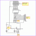
I have this chinese made step motor driver which I would like to control through the LPT port on my PC for CNC work. The software is mach3. The driver is opto-isolated and needs clock and direction signals to drive each axis. But the LPT pulses don't seem to be able to supply enough current to do the job. Some sort of a buffer circuit is needed but exactly what, I don't know. Is there such a circuit ready made which can be purchased or does anybody have any idea how to make such a buffer. It needs to have at least six channels. It also needs to have some sort of protection to prevent possible damage to the LPT electronics. What is such a device called? I don't seem to be able to search for anything useful, so I think I am not using the right jargon in my searches. Thanks for any leads in this respect.
Cheers, Bluebirdiran
 

eblc1388

Joined Nov 28, 2008
1,542
But the LPT pulses don't seem to be able to supply enough current to do the job.
Are you using the LPT port on a laptop? They do not provide sufficient voltage or current like those on desktop PCs. There are also several LPT modes which user can select in BIOS. Your best choice would be the EPP mode.

Some sort of a buffer circuit is needed but exactly what, I don't know. Is there such a circuit ready made which can be purchased or does anybody have any idea how to make such a buffer. It needs to have at least six channels. It also needs to have some sort of protection to prevent possible damage to the LPT electronics. What is such a device called?
The suitable IC device is called a buffer and its part number is 74HCT244. It has eight channels and offer protection between your printer port and external connected circuit. It will also need a separate +5V supply to function.

However, this assumes that all the signals from your parallel port to the stepper motor controller is output only(i.e. in one direction). Perhaps its best to ask the manufacturer of the driver to clarify this.

Google "74HCT244" to get hold of a data sheet.
 

Thread Starter

Bluebirdiran

Joined Feb 5, 2010
62
Thanks a lot Mr. Chung for your reply.
I am using a PC - NOT a laptop.
I have set the BIOS to EPP but has made no difference.
I need at least 6 outputs to the driver, ie. LPT pin No. 2 and 3 for X and 4 and 5 for Y and 6 and 7 for Z movement and direction control. I also have inputs to the LPT port on pin 10 and 11 which consists of the limit switche circuits that control the table home positin. Others such as emergency stop etc. may be input as well.
Electronics not being my strong point (I am better in the Mechanical field) I would appreciate it if you could be a bit more specific as to implementing the 74HCT244 which you have recommended. A little sketch would be very helpful. Assume you are talking a dummy!! Thanks again
 

eblc1388

Joined Nov 28, 2008
1,542
First you ought to prove that the PC printer port is actually working properly. I have assumed you have already done that via a real printer.

You must have some text/image/photo information regarding the stepper driver itself or signal interface requirement by the driver, i.e. which LPT port pin(s) connections are required. Can you post it so that a circuit diagram for the 74HCT244 can be produced?

You still have to get a 5V supply for the circuit to work. It might be possible to get this +5V from game port or PS2 port of the PC or even from the stepper motor driver board if there is one.

If you want 6 outputs and 2 inputs, the circuit arrangement will be different to 7 outputs and 3 inputs because the signal has to go somewhere to the LPT port pins.
 

BMorse

Joined Sep 26, 2009
2,675
these are the typical connections of a 3 Axis (up to 4) CNC to a parallel port... atleast this is how I have mine setup, I do not use mach3 much, I am still using KCam...

Parallel Port Pin Functions using port &H378
Pin/ I/O/ ADDRESS/ BIT/ STATE/ STEPPER CONTROLS

1 O &H37A 0 INVERTED SPINDLE RELAY
2 O &H378 0 NORMAL X-STEP
3 O &H378 1 NORMAL X-DIR
4 O &H378 2 NORMAL X-ENABLE
5 O &H378 3 NORMAL Y-STEP
6 O &H378 4 NORMAL Y-DIR
7 O &H378 5 NORMAL Y-ENABLE
8 O &H378 6 NORMAL Z-STEP
9 O &H378 7 NORMAL Z-DIR
10 I &H379 6 NORMAL NU
11 I &H379 7 INVERTED X-HOME SWITCH
12 I &H379 5 NORMAL Y-HOME SWITCH
13 I &H379 4 NORMAL Z-HOME SWITCH
14 O &H37A 1 INVERTED Z-ENABLE
15 I &H379 3 NORMAL NU
16 O &H37A 2 NORMAL M CODE FUNCTION
17 O &H37A 3 INVERTED M CODE FUNCTION
18-25 GROUND
 

Thread Starter

Bluebirdiran

Joined Feb 5, 2010
62
Mr. Chang
Yes the printer port works ok. In fact I had made a interface using the ULN2803 and everything was ok and all of a sudden without any visible accident the board's cupper got blown off the back of the PCB and it in fact damaged pins 2 and 4 of the printer port. But through the software I have assigned pins 6 and 7 to replace 2
 

Thread Starter

Bluebirdiran

Joined Feb 5, 2010
62
Mr. Chang
Yes the printer port works ok. In fact I had made a interface using the ULN2803 and everything was ok and all of a sudden without any visible accident the board's cupper got blown off the back of the PCB and it in fact damaged pins 2 and 4 of the printer port. But through the software I have assigned pins 6 and 7 to replace 2 and 4. I am attaching the information sheet for the driver. I am using one of these for each axis. If you want to design a board for me, you can design it with more inputs and outputs that the required minimum. I may want to add a fourth axis in the future. These drives are opto-isolated internally and that is the what is causing my troubles, because the opto-isolators draw a lot of current. I think an independant voltage source of 5 volts would be the right choice so as not to intefere with the internals of the motherboard.
Thanks a lot
 

Attachments

eblc1388

Joined Nov 28, 2008
1,542
In fact I had made a interface using the ULN2803 and everything was ok and all of a sudden without any visible accident the board's cupper got blown off the back of the PCB and it in fact damaged pins 2 and 4 of the printer port. But through the software I have assigned pins 6 and 7 to replace 2
It is possible that some other part of the parallel port control IC on the PC motherboard has been damaged in the process. :confused:

From the pdf data sheet you have just posted, to control each stepper motor, three(3) output signals and one(1) input signal from the LPT is needed. Therefore a normal good LPT port can control at most four motors, with 12 output signals and 4 input signals. However, you already have two of the LPT port pins damaged so are now left with only 10 output signals from the LPT port. I doubt you can add a 4th drive to it.

The ULN2803 is the correct part to use for driving the step driver and it should not blow up your interface circuit. Looks like your connection is wrong somehow.

It would be easier to locate what you have done wrong in the existing interface than building another interface(using the same ULN2803).

Please post your existing circuit diagram.
 
Last edited:

Thread Starter

Bluebirdiran

Joined Feb 5, 2010
62
Hello Mr. Chung

I am attaching the existing circuit diagram but pls. note the following. Where you see J2, it is actually an array resistor A103J. Pins 1 and 2 of J1 and J5 are inputs for the two axis ( I am only using 2 at the moment) and the output is taken from 1 to 4 on J4. I would prefer a new design as I don't trust this one. It was not done professionally, I think.
Anyway I leave that to you as long as you can give me a robust design.

This interface worked for hours without any problems. Then I switched off and when I returned and switched back on, it did not work any more. On inspection I noticed that the copper connecting the right side of D1 to pin2 of J3 was blown (pls. see the attachment). I hope this information is enough, but pls. feel free to ask me if you need to know anything else.
Thanks a lot
 

Attachments

Thread Starter

Bluebirdiran

Joined Feb 5, 2010
62
Sorry Mr. Chung, I should have said that Q1 is in fact a 5 volt regulator transistor and the diode is a BY399. What is shown in the pdf file is wrong. These are the actual components on the board. Pin 2 of J3 is positive input 12 volts and pin 1 of J2 is common.
 

Thread Starter

Bluebirdiran

Joined Feb 5, 2010
62
Mr. Chung, I did follow up my last post with some more information but it somehow never got to be shown. So I am repeating it again. In the attached pdf file Q1 is in fact a 5 volt regulator transistor (Not 2N5401)and the diode is a BY933 instead of a fast acting diode. (I did not have one at hand). Pin 2 of J3 is where a 12 volt external voltage source is applied.
 

Thread Starter

Bluebirdiran

Joined Feb 5, 2010
62
Dear Alberto, Thank you for showing interest in this. I have attached the layout schematic so you can have a fuller picture of the circiut. As you can see the com terminal of the IC is connected. And the inputs are directed to 1 to 4 and the output is taken from 15 to 18. I think this is how it should be, don't you. If you have reason to believe that it should be otherwise pls. explain.
Thanks a lot
 

Attachments

Thread Starter

Bluebirdiran

Joined Feb 5, 2010
62
Hello Alberto,
J4 is not a parallel connector but a terminal with screws. Individual wires are connected where appropriate by the screws. Mr. Chung has got it write. His annotations are correct.
Bluebirdiran
 

eblc1388

Joined Nov 28, 2008
1,542
Bluebirdiran,

Before I can prepare a schematic, I would like other members to see if my interpretation of the Driver Module signaling scheme is correct.

It is a shame that all these Asian products are severely let down by cryptic translation from native language into english. If they realize that, may be a simple diagram of the input configuration(like all those we have seen on data sheet) will do. A picture worth a thousand words.

I just don't understand why they do not hire someone say from an academic institute to have a quick look at the translation before printing it. On second thought, perhaps they already did.

Please comments on the following:


Attachments

Thread Starter

Bluebirdiran

Joined Feb 5, 2010
62
Dear Mr. Chung
I don't think that you should concern yourself too much with the deatils of the driver. Just imagine you want to design a interface or buffer or whatever it is called, to get some 2.4 - 5 volt TTL signals and beef them up to 5 volts with some respectable current to be able to activate an array of opto-couplers regardless of where the opto's are located. I think this approach may get us to the solution more quickly.
Thanks
Bluebirdiran
 

eblc1388

Joined Nov 28, 2008
1,542
I just want to make absolutely sure about the interface. Here you go, the changed schematic.

There is no reason to use voltage higher than +5V so I have changed the '+' connections to the step drive module to +5V instead of +12V.

There is no need for the pullup resistor array as there are already pulldown resistors inside the ULN2803. So I have removed it.

This +5V is obtained from 7805 voltage regulator and I have also added a 0.1uF capacitor at the output. This is required to prevent instability of the voltage regulator.

The schematic has been prepared assuming a GOOD parallel port, so if some of your pins are faulty, just use any others from pin#2 to pin#9 to drive the ULN2803 via J1 and J5.

I hope the modified schematic is clear enough for you to proceed and with some care you can perform the modification on the existing PCB and not requiring to build another new one.

If you have questions, please ask in forum.


Attachments

Thread Starter

Bluebirdiran

Joined Feb 5, 2010
62
Hi Mr. Chung

Thanks a lot for all your efforts. For the past couple of days I was waiting for your reply but I was silly enough not to realize that I had to turn to page 3 on the forum :mad:

You say:There is no reason to use voltage higher than +5V so I have changed the '+' connections to the step drive module to +5V instead of +12V.
Can you explain this pls. The step motors coils have to be driven by a voltage higher than 12 volt or there abouts. But I am only usnig the same source but lowering it to 5v for the buffer circuit.
Pls. explain what you mean.
 

eblc1388

Joined Nov 28, 2008
1,542
You say:There is no reason to use voltage higher than +5V so I have changed the '+' connections to the step drive module to +5V instead of +12V.
Can you explain this pls.
My comment about the +5V usage applies to the signalling side only. Its magnitude has nothing to do with driving the stepper motor coil. You should use +24V or +15V or +12V (rated accordingly to your stepper motor) to drive your stepper motor but the signalling can still be done with +5V between LPT port and module.
 

Thread Starter

Bluebirdiran

Joined Feb 5, 2010
62
Yes, but 12 volts was not applied to the signaling side from the begining anyway. 12volts is only taken from the motor side to feed into the 5 volt regulator on the buffer circuit. The only problem with this is that the ground wires will be common to both the signaling and power sides. Can this cause any problems? If yes, should I isolate the 2 power supplies completely by using a lets say 6 volt rectified source for the signaling side and the existing 12 volt source for the motor side.
By the way I will be away for 4 days starting tomorrow morning, I hope to have more of this interesting discussion when I am back but let me express my appreciation for your good work and patience. Thank a lot mate.
Bluebirdiran
 
Top