Facebook
 Google
 GitHub
 Linkedin

I'm trying to wrap up a PCB layout for a client who insists the DRC should have no errors or warnings, however irrelevant they are.  All is fine except for 1 last warning and I can't find the source of it, see screenshot of dialog:
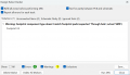
I get what the warning is telling me - I just can't find where it thinks an SMD part expects 'Through hole' pads. The part in question is the TI 74HC4067 which is in the KiCAD library with both SOIC-24 and TSSOP-24 footprints. However I'm using the VQFN-24_EP2 variant of the chip which isn't in the library. So I modified the symbol to add the 25th 'pin' for the thermal pad, changed the part # to add the RGYR (VQFN package) suffix and added the part to my project library and then assigned the TI RGYR VQFN24_EP2 footprint from the footprint library to the part. All was well til I ran the DRC and this violation pops up! I can't find anywhere any reference to through hole pads, everywhere I've looked says SMD. What am I missing? Its seriously doing my head in... and I need to get this out of the door like yesterday1
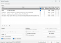
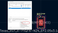
All is fine except for 1 last warning and I can't find the source of it, see screenshot of dialog:I get what the warning is telling me - I just can't find where it thinks an SMD part expects 'Through hole' pads. The part in question is the TI 74HC4067 which is in the KiCAD library with both SOIC-24 and TSSOP-24 footprints. However I'm using the VQFN-24_EP2 variant of the chip which isn't in the library. So I modified the symbol to add the 25th 'pin' for the thermal pad, changed the part # to add the RGYR (VQFN package) suffix and added the part to my project library and then assigned the TI RGYR VQFN24_EP2 footprint from the footprint library to the part. All was well til I ran the DRC and this violation pops up! I can't find anywhere any reference to through hole pads, everywhere I've looked says SMD. What am I missing? Its seriously doing my head in... and I need to get this out of the door like yesterday1
Last edited: