Facebook
 Google
 GitHub
 Linkedin

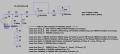
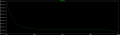
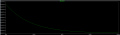
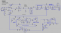
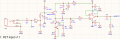
I've been working on an acoustic guitar preamp for some time now, here is one previous thread. The front end is similar to a Fishman Mini (attached). I have measured THD+N using REW and a Motu M4 on various prototypes, both thru hole versions use same JFET BJT arrangement as Fishman mini. SMD version(s) attempted to make it more compact and eliminate hookup wires since they can be a source of noise pickups for a JFET front end. But the THD+N is going up, not down.
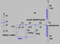
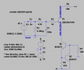
The above measurements are the entire pedal, but for the SMD versions I can measure just the JFET and Buffer portion, same as schematics below:
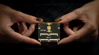
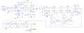
Even though v1.0 is the best, it is clear to me that for v1.0 and v1.1 I didn't know what I was doing with biasing the JFET for lowest noise. I have LTspice and have various simulations, but I am a novice and don't understand how to do noise measurement analysis . So I'm looking for an education on how to properly bias and design a JFET audio front end so it produces the lowest THD+N. I'd love to get THD+N down to 0.01%. Other circuit suggestions are welcome too, but I suspect the JFET is the main thing. The circuit below is roughly 1/2 of the total circuit, the other 1/2 has lots of RC filtering, EQ, etc, recent pictures of v1.0 here.
Vcc, Vee are +-15v using TEC 2-0923 DC-DC converter from 9v.
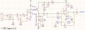
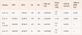
- Original thru hole (Blue), PN4392 and 5088s - 0.058% THD+N
- Next thru hole (Red), PN4392 and 5088s - 0.042%
- SMD v1.0, J113 and SS8050 - 0.028%
- SMD v1.1, MMBF4392 and BC847C - 0.063% (all 4 measured at same level)
The above measurements are the entire pedal, but for the SMD versions I can measure just the JFET and Buffer portion, same as schematics below:
- v1.0 power board only - 0.0096% THD+N
- V1.1 power board only - 0.059% THD+N
Even though v1.0 is the best, it is clear to me that for v1.0 and v1.1 I didn't know what I was doing with biasing the JFET for lowest noise. I have LTspice and have various simulations, but I am a novice and don't understand how to do noise measurement analysis . So I'm looking for an education on how to properly bias and design a JFET audio front end so it produces the lowest THD+N. I'd love to get THD+N down to 0.01%. Other circuit suggestions are welcome too, but I suspect the JFET is the main thing. The circuit below is roughly 1/2 of the total circuit, the other 1/2 has lots of RC filtering, EQ, etc, recent pictures of v1.0 here.
Vcc, Vee are +-15v using TEC 2-0923 DC-DC converter from 9v.
Attachments
-
 96.8 KB Views: 5
Last edited: