Designing a Delayed MOSFET switch Circuit for Voltage Transfer on a PCB

Thread Starter

DvirIL

Joined Nov 2, 2020
29
I am seeking guidance for the design of a circuit on a PCB board. The intended function of this circuit is to facilitate the transfer of a 24 V voltage from the input to the output through the utilization of a load switch (SIP32429DN (datasheet), 3 A maximum). This transfer should only occur when a designated button is pressed.

Upon releasing the button, my objective is to sustain the circuit's activity for an additional second before initiating closure. In other words, I aim to introduce a brief delay before the circuit deactivates, rather than an immediate cessation upon button release.

could you give me another solution that will be simple and work?(without MCU)
this is what I think but The load switch not good solution because the internal pull-down could change the value significantly
1693726793562.png
 

Jerry-Hat-Trick

Joined Aug 31, 2022
446
I may have got this wrong, having only looked at the device specification briefly, but if your push button is connected on one side to the 24V and the other side to two equal value resistors in series to ground, with a capacitor across the two resistors and a 5V zener diode across the resistor going to ground, pressing the button should give you the 5V you need to enable the device and it will remain at 5V until the the voltage across the capacitor drops below 10V. Maybe try 2 x 1K resistors and try different capacitor values, or do the calculations!
 

LowQCab

Joined Nov 6, 2012
3,580
If You would explain in detail why You want to do this,
and exactly what it is supposed to accomplish,
and supply us with a proper Schematic diagram of your project,
You might then get some more useful suggestions.
.
.
.
 

Thread Starter

DvirIL

Joined Nov 2, 2020
29
If You would explain in detail why You want to do this,
and exactly what it is supposed to accomplish,
and supply us with a proper Schematic diagram of your project,
You might then get some more useful suggestions.
.
.
.
I'm working on designing a circuit board that regularly receives a 24-volt input. Additionally, there's an external button that can either connect or disconnect a 20V supply to the board. The board incorporates three PMOS FETs and a BJT transistor.

The FETs' source terminals are connected to a constant 24V supply, and the BJT's base terminal is linked to the button through a voltage divider or any other appropriate method suggested in your proposal.

My objective is to ensure that when someone presses the button, the transistors turn on immediately. However, a crucial aspect of this operation is ensuring that once the button is released, it genuinely stays in the off-state for safety reasons. To accomplish this, I'd like to provide the user with approximately half a second from the moment they release the button to verify that there is no voltage at the base of the BJT.

using a load switch might be suitable because it may not pass the 24V supply to the board(24V->24V_FET). How can I achieve this functionality effectively?
 

LowQCab

Joined Nov 6, 2012
3,580
Schematics ?
Pictures ?
Explanation of Purpose ?

1 accurate Schematic is worth at least a hundred word-salad posts.

You need an evaluation of the suitability of a proposed project designed a particular purpose.
.
.
.
 

Thread Starter

DvirIL

Joined Nov 2, 2020
29
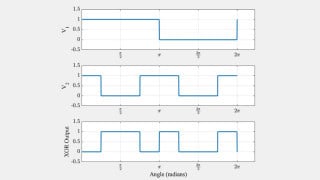
I have 24v Input from push button, I want to make delay when I leaved the button and the PMOS will stay on for about 0.6sec. attaching some timing diagram for the required operation signals(pay attention when 24v goes to zero means its disconnected,someone release the button): enter image description here

  • input:meaning the button was pressed the voltage will be 24v or open
  • I want that black box will charge fast(0-40ms)
  • when I release the button, I want the black box will hold the voltage for about 0.6sec and the output will stay high means that PMOS will stay ON. I saw some idea about this circut to use some Comprator(e.g the blackbox will be comprator)(question):
enter image description here

but I have a couples of issues with this circuit:

  • I want another discharge time(maybe some diode with another discharge route?)
  • the SOURCE of my PMOS should be 24V so the margin will be very narrow
  • the current PMOS should drive will be about 3Amp
  • I want that will be in architecture High-Side Switch so that why I chose PMOS
  • its okay to use some voltage divider before the comparator (voltage divider to push-button) but I need to switch 24V to another stage 24v_FET.
should I use another BJT after the comprator? should I use comprator at all? I have another 3.3v in my circuit from another supply so can I use it if you see some need.
 

Thread Starter

DvirIL

Joined Nov 2, 2020
29
Schematics ?
Pictures ?
Explanation of Purpose ?

1 accurate Schematic is worth at least a hundred word-salad posts.

You need an evaluation of the suitability of a proposed project designed a particular purpose.
.
.
.
see the new post
 

crutschow

Joined Mar 14, 2008
33,346
input:meaning the button was pressed the voltage will be 24v or open
That seems contradictory.
What voltage?
When the button is pressed do you want the MOSFET ON or OFF?
Note that when the P-MOSFET gate voltage is high, the MOSFET is off.
 

LowQCab

Joined Nov 6, 2012
3,580
Now we're starting to get some good information,
but there are very important things that are still being omitted.

1) What is the "Problem" that this Delay-Circuit supposed to solve ?

2) What Load is being Switched by the FET ?

3) How much Current does the Load require ?

4) Is the Load ...... Inductive / Resistive / Capacitive ?

5) Why does the FET need to remain ON for ~0.6-seconds after the Push-Button is released ?

6) Is the Time-Delay critical ?, How precise must the Time-Delay be ?, and why.

7) Would it be an advantage to make the "Off-Delay" time adjustable ?

8) Why is the Input-Voltage from the Push-Button ~24-Volts, but the FET is Switching ~5-Volts ?

9) What is supplying the ~5-Volts ?

10) What is supplying the ~24-Volts ?

11) What is the meaning of "Voltage-Transfer" ?, dose this simply mean an On/Off Power-Switch ?
.
.
.
 

crutschow

Joined Mar 14, 2008
33,346
If I understand your requirements correctly, below is the LTspice sim of a simple circuit that should work for you:
The output turns on immediately (<2ms) (yellow and red traces) when the push-button is pressed (green trace) with about a 0.6s delay after the push-button is released.

Due to component tolerances, you may have to tweak the value of R3 (also could use a 500k pot in series with a 200kΩ resistor for R3) to get the off delay within your time requirements.
M2 can be just about any P-MOSFET with a ≥40V rating and an on-resistance of ≤50 milliohms.
C1 should be a ≥50V film type capacitor, not an electrolytic (aluminum or tantalum).
A ceramic cap may be acceptable, but they have poorer tolerance and temperature coefficient than film types.

If you want to control more than one MOSFET output from the same PB, just connect the additional P-MOSFET's gates to M1's gate.

(Edit: Added R5 to keep M2's Vgs below 20V.)

1694104071608.png
 
Last edited:

Thread Starter

DvirIL

Joined Nov 2, 2020
29
If I understand your requirements correctly, below is the LTspice sim of a simple circuit that should work for you:
The output turns on immediately (<10μs) (yellow and red traces) when the push-button is pressed (green trace) with about a 0.6s delay after the push-button is released.

Due to component tolerances, you may have to tweak the value of R3 (also could use a 500k pot for R3) to get the off delay within your time requirements.
M2 can be just about any P-MOSFET with a ≥40V rating and an on-resistance of ≤50 milliohms.
C1 should be a ≥50V film type capacitor, not an electrolytic (aluminum or tantalum).
A ceramic cap may be acceptable, but they have poorer tolerance and temperature coefficient than film types.

If you want to control more than one MOSFET output from the same PB, just connect the additional P-MOSFET's gates to M1's gate.

View attachment 302237
your solution is extacly what I want, but what about M2, im looking in datasheet and max VGS 20v !
so how do you apply 24v to gate ? what am I miss here?
 

crutschow

Joined Mar 14, 2008
33,346
what about M2, im looking in datasheet and max VGS 20v !
so how do you apply 24v to gate ? what am I miss here?
You are apparently missing a proper understanding of the voltage divider effect caused by R1 and R2 in generating the value of Vgs.
[Note that it is the (relative) gate-to-source voltage, Vgs, not the gate-to-ground voltage, that is the primary voltage of interest here.]
So Vgs is a maximum of 1/2 the supply voltage (12V) when M2 is on, and 0V (Vg=24V) when M2 is off.

Below is the sim showing M1's drain-ground voltage (Vd, blue trace), M2's gate-ground voltage (Vg, red trace), and M2's gate-source voltage (Vgs, yellow trace).

Make sense now?

1694104841892.png
 
Last edited:

Thread Starter

DvirIL

Joined Nov 2, 2020
29
You are apparently missing a proper understanding of the voltage divider effect caused by R1 and R2 in generating the value of Vgs.
[Note that it is the (relative) gate-to-source voltage, Vgs, not the gate-to-ground voltage, that is the primary voltage of interest here.]
So Vgs is a maximum of 1/2 the supply voltage (12V) when M2 is on, and 0V (Vg=24V) when M2 is off.

Below is the sim showing M1's drain-ground voltage (Vd, blue trace), M2's gate-ground voltage (Vg, red trace), and M2's gate-source voltage (Vgs, yellow trace).

Make sense now?

View attachment 302290
You edit the value of R4, the first value was 20 ohm, am I wrong?
 

crutschow

Joined Mar 14, 2008
33,346
You edit the value of R4, the first value was 20 ohm, am I wrong?
Nope, not wrong.
Since I added R5 which forms a voltage-divider to reduce M2's maximum gate voltage, I then increased its value to reduce the quiescent power.
For your purposes, that change has only a negligible effect on the circuit operate time.
 
Last edited:

Thread Starter

DvirIL

Joined Nov 2, 2020
29
Nope, not wrong.
Since I added R5 which forms a voltage-divider to reduce M2's maximum gate voltage, I then increased its value to reduce the quiescent power.
For your purposes, that change has only a negligible effect on the circuit operate time.
thanks again,
the voltage that need to open/close the gate of M2 is the Vgs threshelod? because the discharge time should be the time take from 24v to vgs(th) not from 24v->0v, am I wrong?
because if I get you correct , the Tau constant time to discharge is 442k*1u=0.442Sec, but after this time the voltage on gate will be 0.33*24(8v)
 

crutschow

Joined Mar 14, 2008
33,346
the voltage that need to open/close the gate of M2 is the Vgs threshelod?
Yes.
But please use the proper terms.
The voltage on the gate is what controls the MOSFET "channel", the "gate" is just the name for that terminal, it is not open/closed.
So it is the channel that is open/close (non-conducting/conducting or off/on).
the discharge time should be the time take from 24v to vgs(th) not from 24v->0v, am I wrong?
That is correct.
the Tau constant time to discharge is 442k*1u=0.442Sec, but after this time the voltage on gate will be 0.33*24(8v)
Technically closer to 0.368 x 24V = 8.8V

See below for the sim of an RC circuit with a 1 second Tau:

1694358741238.png
 
Last edited:

Thread Starter

DvirIL

Joined Nov 2, 2020
29
Yes.
But please use the proper terms.
The voltage on the gate is what controls the MOSFET "channel", the "gate" is just the name for that terminal, it is not open/closed.
So it is the channel that is open/close (non-conducting/conducting or off/on).
That is correct.
Technically closer to 0.368 x 24V = 8.8V

See below for the sim of an RC circuit with a 1 second Tau:

View attachment 302489
Thanks for the informative answers.
By the way, why the capacitor should be film capacitor and not tantalum or aluminium?
 
Last edited:

crutschow

Joined Mar 14, 2008
33,346
By the way, why the capacitor should be film capacitor and not tantalum or aluminium?
Because tantalum and aluminum capacitors have significantly higher leakage currents, and worse capacitance value tolerances.
The are fine for filtering in power supplies, but not so much for timing circuits if the time period accuracy is important.
 

Thread Starter

DvirIL

Joined Nov 2, 2020
29
Because tantalum and aluminum capacitors have significantly higher leakage currents, and worse capacitance value tolerances.
The are fine for filtering in power supplies, but not so much for timing circuits if the time period accuracy is important.
I'm looking for film capacitor and found only TH and not SMT , the PCB assembly house should be ok with TH capacitor? they know how to handle with TH capacitor? it looks me strange
 
Top