I prefer to use "re ≈ 26mV/Ic" to express the voltage gain.
\(\Large \frac{Vout}{Vin} = \frac{Rc}{re + \frac{R_B}{Hfe +1}}\)
And LvW is correct. It turns out that the person who made a small mistake is you not LvW.
I prefer to use "re ≈ 26mV/Ic" to express the voltage gain.
\(\Large \frac{Vout}{Vin} = \frac{Rc}{re + \frac{R_B}{Hfe +1}}\)
And LvW is correct. It turns out that the person who made a small mistake is you not LvW.
To be hones I wrote this gain formula by inspection.
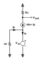
I simply remember that the voltage gain for CE and CB amplifier is equal to Av ≈ Rc/re (the only differences is minus sign - 180 phase shift )
And I also know that Rb is seen at emitter as RB/(Hfe + 1). So finally Av ≈ Rc/(re + Rb/(hfe + 1))
Of-course we can use small-signal T model to find out the voltage gain for CE amplifier
Sorry about that. Hope you don't angry. It is me who made mistake but I edited that.
Jony,
If I understand your post correctly, you are calculating voltage gain of common base from common emitter?
I understand your calculations in both cases, common emitter and Rin. However, I don't know how can you combine Rin and common emitter to get the formula Av ≈ Rc/(re + Rb/(hfe + 1)).
I think you converted base emitter RB into emitter branch.
RB => RB/(Hfe +1)
I can't figure out why this works. The small signal models of two topologies are different and don't know how to transform one to the other.
Voltage gain for CE stage = the total load resistance seen at the collector divided by "re" plus the total resistance placed in series with "re" (emitter). And RB/(Hfe +1) is in series with "re".
Hi Joni - excuse me, it is really not so important: Nevertheless, I am interested to hear WHY you prefer "re" instead of 1/gm ?
To me, the transconductance gm has a physical meaning - it is simply the small-signal ratio Iout/Vin (to be interpreted as a slope of the Ic=f(Vbe) characteristic.
And what is the meaning/interpretation of "re"?
I appreciate that everybody has its own preferences - nevertheless it is interesting to learn something about the background.
Yes you will still have a common base topology. But without Cdec capacitor the base voltage divider resistors will be seen at the emitter as a (R1||R2)/(Hfe + 1).
This is where I don't understand. Can you tell me how to do that? I mean how can I convert RB from that branch to emitter branch and how to calculate the resistance added in emitter?
Hi Joni - excuse me, it is really not so important: Nevertheless, I am interested to hear WHY you prefer "re" instead of 1/gm ?
To me, the transconductance gm has a physical meaning - it is simply the small-signal ratio Iout/Vin (to be interpreted as a slope of the Ic=f(Vbe) characteristic.
And what is the meaning/interpretation of "re"?
I appreciate that everybody has its own preferences - nevertheless it is interesting to learn something about the background.
As you might know or not I'm hobbyist, not a professional EE.
And when I first start reading about BJT amplifier back in 1998 I was introduced to the concept of a current source and current control hydraulic BJT model. Next was CC amplifier and CE amplifier with emitter degeneration resistor. And I was taught that CE stage gain is equal to Rc/Re. Next I find out that even if we short emitter to ground, there is still emitter resistance built-in into emitter. The ideal transistor with intrinsic emitter resistance "re = 26mV/Ic". And all these things were taught without any semiconductors physics and small-signal transistor model.
It was completely based on an intuitive approach. The art of electronics also use similar approach. And this is why I prefer "re" instead of gm.
This is where I don't understand. Can you tell me how to do that? I mean how can I convert RB from that branch to emitter branch and how to calculate the resistance added in emitter?
Jony, as I remember from the first days joining the site you helped me how currents flow in a circuit. I didn't have any idea how a current makes a complete journey before, even I have learn EE for many years. You have helped me a lot! I wasted a lot of time but I am trying to catch up.
anhhnha, perhaps there is a misunderstanding because joni`s formulation is not quite clear.
Nothing is "converted to the emitter branch".
What he means (and this is fully correct) is the following:
The input resistance as can be seen from the emitter node into the transistor must, of course, also contain some external circuitry that is connected to the base (because there is a conducting path between E and B). That`s all.
And I was taught that CE stage gain is equal to Rc/Re. Next I find out that even if we short emitter to ground, there is still emitter resistance built-in into emitter. The ideal transistor with intrinsic emitter resistance "re = 26mV/Ic".
Joni, thank you for explaining your position.
It is not my task and my intention to force you leaving this way of understanding - nevertheless, may I ask you some questions?
Perhaps it helps.
* Did you ever try to understand why the gain of a CE stage is -Rc/Re ?
(by the way: Don`t mix symbols for ohmic resistors and differential small signal resistances: It should read -Rc/re)
* More than that, did you ever try to find the place within the BJT where this "resistor" is located? Has a pn diode such a resistor? Why not? Why is this "resistor" depending on Ic?
* Don`t you agree that it sounds logical to say that an input small-signal voltage v,be is converted to a small-signal current i,c because the transistor is a voltage controlled current source?
And the conversion factor is simply the transconductance i,c/v,be=d(Ic)/d(Vbe)=gm ?
* This gives the gain (for RE=0): -gm*Rc.
* What is the physical background of re=Vt/Ic ?
The explanation is based on the transconductance gm=d(Ic)/d(Vbe) which is nothing else than the slope of the control characteristic Ic=f(Vbe). Because of the exponential function involving Vbe and Vt the slope is gm=Ic/Vt.
(You know, the notation re=1/gm is just an attempt to use only resistances within a formula. But - for my opinion - this works against a good understanding about whats really going on).
_________________
This is my view and my approach to understand the working principle of BJT`s. I hate to use formulas without knowing the physical background.
LvW
 Facebook
 Google
 GitHub
 Linkedin