De-bounce circuit not working as expected

Thread Starter

recklessrog

Joined May 23, 2013
985
upload_2018-6-13_21-34-45.png

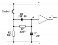
I have been trying to de-bounce some tactile switches and after testing several ideas I came across this circuit that only works if R2 is between 470r-1k. as it is, the 4027 changes state while the push button is depressed, but reverts as the button is released. Supply voltage is 10 volts.

I have tried swapping the position of r2 and the push button so that it changes state on release, but again, that only works when r2 is 1k or less.

Oscilloscope shows that the switch is de-bounced. I have tried grounding all the other inputs for the second flip flop in the chip, and wiring it in the same way. Again, it works fine if r2 is 1k or less.

Oh, yes there is lots of proper decoupling of the ic, a 100n and 2.2mfd tant right on the supply pin.
 

Attachments

Last edited:

AnalogKid

Joined Aug 1, 2013
11,055
the 4027 changes state while the push button is depressed, but reverts as the button is released.
That is the definition of a debounced SPST switch. Without getting into that particular circuit, what is it you want the circuit outputs to do?

Can you post a link to the source of that circuit?

ak
 

danadak

Joined Mar 10, 2018
4,057
If you need to do more than just debounce some devices have a debounce
HW facility in them. Just some of the stuff in the part -

upload_2018-6-13_19-16-47.png

You can have multiple debouncers.

As an aside part handles CapSense for input switches, eliminating mechanical
switches, and they "effect" debounce internal to them.

Regards, Dana.
 
Last edited:

ebp

Joined Feb 8, 2018
2,332
Although the circuit at #1 filters out the bounce, it still produces an output signal that falls fairly slowly as the capacitor discharges. The clock input of the flip flop therefore spends a good deal of time within a voltage range that is "undefined" - higher than a guaranteed logic "0" but lower than a guaranteed logic "1". The reality is that most CMOS devices will take anything just a bit lower than half of the supply voltage as LOW and anything a bit higher as HIGH. Slowly passing through that zone makes it possible for even a small amount of noise to cause an unwanted state change.

When you use an RC filter, its output should go to a Schmitt trigger device that has input hysteresis. No voltage that falls anywhere between the supply rails is undefined. For an input voltage to be considered HIGH it must be above certain threshold. Once the voltage has reached that threshold, the input will still be treated as a clean logic HIGH until it falls to a lower threshold, where it is treated as LOW. This behavior allows the device to always produce clean output logic levels even with slowly changing input voltage. It also means that noise has to be great enough in amplitude to cross the "opposite" threshold to cause any problem.

Sometimes it is a good idea to include a resistor in the circuit between the cap and the switch to limit the peak current. With a small cap the transient current peak is very short, but it can still be enough to eventually cause damage to silver or gold plating on contacts.

The CD40106 as shown in dl324's circuit is an inverting Schmitt trigger. The CD4093 is a quad 2-input NAND Schmitt trigger. Some of the 4000 series ripple counters with a bunch of stages have hysteresis on the clock input. I don't know of any flip-flop in any series with built-in hysteresis on the clock.

Some flip flops rely on an internal delay to produce the required temporal separation of input and output events. If the clock rise or fall time is too slow, the delay can be defeated and the circuit misbehaves. Some devices specify a maximum allowable rise and/or fall time.
 

crutschow

Joined Mar 14, 2008
34,460
The problem with a debounce circuit on the FF clock input is that it can slow down the risetime, and most FF's require a fast risetime for proper operation.

Here's the circuit I prefer for a FF debounce:
It has a delay in the feedback to prevent changing states more than once during the switch bounce time.
The switch is connected to V+.

Unfortunately it does not work with a JK FF unless you add an inverter or use two RC delay circuits.

upload_2018-6-13_16-23-36.png
 

AnalogKid

Joined Aug 1, 2013
11,055
The CD40106 is a great debounce part, but it is a lot of unused pins if you have only one switch. Consider an opamp or two-transistor circuit for low switch count applications.

CD4093 - 4 switches
LM339 or LM324 - 4 switches
LM393 or LM358 - 2 switches
2 transistors, any single opamp (with the appropriate input and output voltage ranges), or a 555 - 1 switch

https://images.search.yahoo.com/sea...wNwaXZz?p=schmitt+trigger+circuit&fr2=piv-web

ak
 

crutschow

Joined Mar 14, 2008
34,460
It's not clear to me if the TS wants a debounced alternate-action (FF) circuit for the PB switch, or just a debounce circuit for the switch. :confused:
 

AnalogKid

Joined Aug 1, 2013
11,055
It sounds to me like debouncing a normal SPST momentary switch and synthesizing alternate-action for the output, a debounced toggle circuit, but only the TS knows.

ak
 

danadak

Joined Mar 10, 2018
4,057
How many switches do you have to do and what happens to their output,
what is the switch signal used for ?

Regards, Dana.
 

Thread Starter

recklessrog

Joined May 23, 2013
985
Here is the article that went with the circuit. It is basically to toggle the outputs on alternate pushes of the momentary push button. The outputs are then used as steering control inputs to a 4066 bilateral analogue switch.


The circuit uses a few simple components to
remove the contact bounce. When the push switch
is open, the voltage at point A is held low through
R1 and R2 and C1 is discharged. Pressing the
switch causes C1 to charge rapidly through D1,
bypassing R1. This causes point A to go high fairly
rapidly.
When the switch is released, the voltage at
point Acan't fall quickly as it is held up by the charge
stored in C1. The capacitor can only discharge
through R1 and R2 in series as D1 is now reverse
biased. The switch contacts have time to bounce
and separate cleanly before the voltage on C1 falls
significantly.
The output at point A should be connected to a
suitable logic gate to 'square up' the edges of the
output.
Push On, Push Off Switch Circuit
A further development of the above circuit is to
connect the output to a J-K flip-flop. This provides a
circuit where the output alternates between on and
off at each successive push of the switch. The circuit
uses half of a 4027 flip-flop IC - the IC contains two
separate but identical flip-flops which share common
power supply connections. each flip-flop has two
outputs which complement each other. ie. one output
is always the inverse of the other.
The circuit shown is triggered on the leading edge of
the switch pulse. This means that the outputs
change as the switch is pushed. The circuit may be
modified to operate as the switch is released by
swapping the positions of the switch and R2.
 

crutschow

Joined Mar 14, 2008
34,460
C1 is too small to give sufficient debounce time (1ms time constant).
Try a C1 value of 0.5-1μF instead.

Or try the circuit in post #6.
 

Thread Starter

recklessrog

Joined May 23, 2013
985
C1 is too small to give sufficient debounce time (1ms time constant).
Try a C1 value of 0.5-1μF instead.

Or try the circuit in post #6.
Thanks, Yes the 4013 does seem easier to use, problem is I have twenty 4027's and only one 4013 and none of my local suppliers have the 4013 in stock. I will try changing C1.
 

ericgibbs

Joined Jan 29, 2010
18,865
hi Roger,
The early versions of the 4013 did not have a Schmitt Clock input, later versions do now have a Schmitt Clock.
E

EDIT:

Your 4027 J/K should be connected as this image, if you want alternate F/F clock action.
 

Attachments

Last edited:

Thread Starter

recklessrog

Joined May 23, 2013
985
hi Roger,
The early versions of the 4013 did not have a Schmitt Clock input, later versions do now have a Schmitt Clock.
E

EDIT:

Your 4027 J/K should be connected as this image, if you want alternate F/F clock action.
Thanks Eric, I will try that later.
 

Thread Starter

recklessrog

Joined May 23, 2013
985
hi Roger,
The early versions of the 4013 did not have a Schmitt Clock input, later versions do now have a Schmitt Clock.
E

EDIT:

Your 4027 J/K should be connected as this image, if you want alternate F/F clock action.
Hi Eric, I tried that circuit and again it only works if the resistor is 1k or less. I noticed that yours shows a 5v supply and I am using 10V.
something strange is going on because I've tried different values for the capacitor as well. :(
 

ebp

Joined Feb 8, 2018
2,332
"The early versions of the 4013 did not have a Schmitt Clock input, later versions do now have a Schmitt Clock."

The TI, ST and ON parts don't have a Schmitt trigger for the clock. The HEF4013 from Nexperia does. Same for 4027.

Nexperia has been quietly changing a bunch of specs for their 4000 series - many are much faster than those from other manufacturers. This must make it "fun" for designers who spec the HEF parts, write careful notes saying "no substitution because ..." and have said notes ignored by some putz who thinks he knows better.

D1 and R1 in the original circuit at #1 serve no useful purpose if used together. The diode undoes what the original intent of R1 probably was in the circuit partially copied by the "designer" of the variant - limiting the peak charging current to protect the switch contacts. Since there is nowhere for current to go during cap discharge other than R2 and since the contribution of R1 to slowing discharge is negligible, D1 is useless for anything related to that aspect. If you don't care about your switch contacts, just omit both R1 and D1 - two components saved for the same result.

Crutschow's circuit at #6 is vulnerable to spurious clocking if the capacitor voltage has settled before the switch opens and there is bounce on opening.
 

AnalogKid

Joined Aug 1, 2013
11,055
There are a looooot of different JK flipflops out there, and eric's circuit in #14 is more reliable than the circuit in #1.

Also, D1 is in backwards in both circuits. Given that current limiting resistor R1 is only 5% of timing resistor R2, and this is not a critical timing situation, I don't think the diode is needed at all. But if it's gonna be in there, it should be oriented to do something useful.

ak
 
Top