Facebook
 Google
 GitHub
 Linkedin
I'm not totally satisfied... I'd like to know whether the other contributors on the thread agree with me that comparing the input transistor to a diode is pointless and confusing, and that the comparison should be removed from the tutorial.
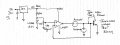
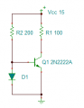
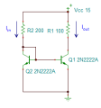
Your explanation sounds pretty simple and obvious but I don't think it is. In my simulation circuit, there is a fixed voltage applied, so it's not simply that a fixed current is now divided between the collector and the base, so the base current must drop.
The current is not limited by the voltage source, and it would be quite possible for the total (emitter) current to increase, with 100 mA collector current and 1 mA base current, if that was how the transistor behaved.
Clearly though, current in the collector-emitter path affects the base-emitter diode's behaviour - for a given, fixed forward voltage, the base-emitter diode draws much less current if there's current flowing from collector to emitter. That is not obvious or simple, although (I assume, from t_n_k's comments) the Ebers-Moll model would predict it.
BTW the collector voltage doesn't have to exceed the base voltage for the effect to occur. If it did, Vce(sat) would be higher than Vbe. I did an LTSpice simulation with a fixed Vbe and a ramping Vce. Ib starts dropping immediately when Vce rises above 0V and has pretty much levelled out by the time Vce has reached +0.2V. That's with a 2N3904.
")