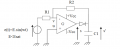
For a positive input the output goes negative (since it's an op amp inverting configuration). This reverse biases the diode so the capacitor voltage remains unchanged.
When the input goes negative, the output goes positive. This forward biases the diode and (due to the feedback through R1 and R2) the capacitor voltage follows the inverse of the input voltage, charging the capacitor to the peak voltage.
When the voltage starts to fall the diode is again reversed biased, thus the capacitor voltage stays at the peak voltage, being discharged slowly by the current through R1 and R2 (not shown in the graph).
Below is an LTspice simulation to show this.
(I added the capacitor across R2 to damp some small oscillations in the simulation).
Note that I inverted the input in the bottom graph [-V(in)] so it corresponds to the inverted output due to the op amp inversion.
V(oa) is the op amp output (it goes to the op amp negative rail when the diode becomes reverse biased due to the opening of the feedback loop).
You can see the small reduction of the capacitor voltage between peaks due to the discharge through R1 and R2.
If you carefully read my post you would have the answer to that question.
Since the capacitor voltage is higher than the zero volts average value of E(t) it will discharge (not charge), as I noted.
The time constant for this is ≈(R1+R2)*C1 = 20k*5μF = 100ms which gives an exponential discharge of about 8.9% of the peak voltage for the 9.3ms between one peak and the start of the next peak's charge.
This is the slight discharge of V(out) between peaks seem in the simulation.
Here is a variation on the peak detector with very very low output droop.
The main purpose for the added components (and some of the existing ones) are:
1. Diode D1 is the normal peak detector diode.
2. Diode D2 prevents discharge of C1 while allowing some temperature compensated feedback.
3. Diode D3 prevents negative output saturation of the op amp during positive input peaks.
4. R3 prevents a high output surge current from the op amp.
5. C1 filter cap.
6. R4 is the presumed load which should be a buffer.
Note the value of R1 or R2 can be changed slightly to get the right DC output which might be desirable since the voltage drop across D2 will be a little more than across D1.
Most notable in the waveforms shown in the attachment are:
1. The output droop is very low.
2. The op amp output negative excursion clamp voltage is less than 1v.
3. The waveforms shown start at approximately 400ms after startup for clarity.
 Facebook
 Google
 GitHub
 Linkedin
 10.3 KB Views: 11
 9.7 KB Views: 9


