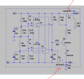
Hello Alec,I am converting the schematics into PCB and choosing components.
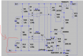
I noticed and issued with the |Vgs| of the mosfets is 12V. This is very hight .
not many mosfets have the ability to wisdand such |Vgs|.
For PMOS it was solved by changing R19 to 40K.
However M1 has Vgs of 14V.
Is there a way to reduce this gate source voltage so thegeneral functionality will be saved and M1 NMOS wont be burned?
LTspice simulation is attached.
Thanks.
You're right about Vgs being too high for that particular MOSFET. My bad. I picked it for the sim out of the LTspice standard library, on the basis of its Vds rating but forgot to check the Vgs rating. Apologies. It seems that particular type is now obsolescent, so not a good choice anyway. You can use whatever MOSFETs you choose, if their parameter ratings are appropriate. You will notice I put 'etc' alongside the M1 and M2 types.
Hello Alec , yes I totally remmember that you said that I choose pick the mosfets.
But all mosfets I saw work with maximal rating Vgs of 8 volts .there is no such mosfets.
Is there some way to update the circuit so it will reduce the Vgs of the NMOS ?(without hurting the functionality )
For Pmos I solved the problem by increasing R19.
Thanks.
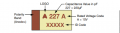
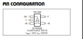
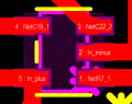
Hello Alec, I chose the following component to be C10.
Its tantalum so its polarised and i need to make sure positive pint Anode + will be always higher then negative pin anode.
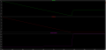
Voltage plots of a cathode anode and anode-cathode shown below.
Two question:
1.So I put the capacitor brown stripe next to R26 and In- to the Cathode?
2.How can i make sure they wont change polarity on a brief moment and burning the capacitor?
Thanks. https://eu.mouser.com/datasheet/2/40/TAJ-3165264.pdf
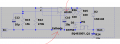
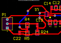
Hello Alec,I have started to implement the lower comperator circuitry as shown below.I am using a 2 layer pcb
However as you can see below i need to route on the GND layer thus i am hurting my GND.
Is there recomendation regarding the optimal way to route this circuit?
Thanks.
Sorry, I'm not familiar with board layout/routing software. I don't think layout is too critical for this particular project though, providing trace widths are adequate for the currents involved.
Hello Alec, I have made the PCB of my sequencer, I need to connect the GND's nets together .They are varius.
I can do polygon pour , I can do direct track routing.
How do you reccomend to connect the GND in this circuit?
PCB and video are attached in the link below.
If you cant open Altium file Is there some alternative PCB format file which I could try to use so you could see my PCB?
Thanks.
Hello Alec_t, I have built the circuit you reccomended and it worked precisely like in the simulation.
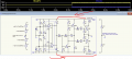
I want to learn the more advanced circuit you proposed as shown below in the photo and attached LTspice file.
Could you please give some intuition regarding the functionality of the part signed by red arrows.
This diode bjt combination looks like magic.
Could you give some intuition so I could investigate their functionality?
Thanks.
Good to hear the circuit performs as expected.
When node e goes high (both suply rails stable), current through R7 and D1 turns on Q1, pulling down Q2 base and turning Q2 on. Q2 collector voltage rises, causing current through R11 and D3 to increase Q1 base current. This positive feedback action speeds up the Q1 switching, thus avoiding any dithering.
Q1 collector voltage turns on Q4. Q2 collector voltage turns on Q3 at the same time.

 Facebook
 Google
 GitHub
 Linkedin