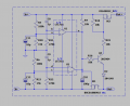
converting power supply signal into pulse signal

Alec_t

Joined Sep 17, 2013
15,132
What could cause it?
You are now asking Q5 and Q6 (in your sim) to provide quite a lot of current, whereas your original post just mentioned providing a pulse. At the very least the base resistors R6/R25 probably need reducing.
Rload1 and Rload2 can be removed.
 

crutschow

Joined Mar 14, 2008
38,598
Which LTS version do you have?
I use the old Version 4.23l as I prefer the interface to the new version, which changed all the short-cut commands.
Perhaps they also changed the generic models so they work better.
But even if they do, I prefer not to use any generic models in my sims.
 

Alec_t

Joined Sep 17, 2013
15,132
I prefer not to use any generic models in my sims.
Fair enough. For circuits where components are in unusual or critical scenarios or are likely to be used near their expected parameter limits I'd do the same as you.
MOSFET default models always seem to cause odd results.
 
Last edited:

Thread Starter

yef smith

Joined Aug 2, 2020
1,472
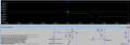
Hello, In the attached load_for_stabilizer positive +12V pulse supplies 90mA while -12 V input pulse supplies 300mA and more at some points as shown in the attached LTspice and photo below.
I increases by 10 times "Rload1 and Rload2" .
I tried to unite both simulations and i get some anomaly (attached united_sim.rar)
out port is +12V but P12 is 1V but they are on the same net.
Why my simulation is not working when i am uniting both circuits?
Thanks.
1728652841996.png
 

Attachments

Alec_t

Joined Sep 17, 2013
15,132
out port is +12V but P12 is 1V but they are on the same net.
Are you saying you have two different labels for the same node?

Edit:
Btw, I've been experimenting with adding ripple to the supply rails in the sim and, as I indicated in post #14, the network at the comparator inputs of my suggested circuit will need modifying to cope. So far I've been unable to come up with a dependable solution for ripple exceeding about 3%. The ripple in your post #1 waveforms appears considerably more than that.
 
Last edited:

Thread Starter

yef smith

Joined Aug 2, 2020
1,472
Hello Alec,I am trying to learn this circuit.
Is there a way to analize this circuit as separated block?
What the different functionality of each block?
So i could simulate one by one and see how the combined result functions?

Also could you please add the ripple simulation file so i could see the problem ?
Thanks.
 

Thread Starter

yef smith

Joined Aug 2, 2020
1,472
UPDATE:

Hello Alec, could please show howincrease the ability to supply current?
you said to reduce"R6/R25".
Is there are more ways to increase the ability to produce current?
Also it would be great if you couldsay how the ripple problem could be handled.
Thanks.
 

Alec_t

Joined Sep 17, 2013
15,132
I'm not aware of a voltage supervisor IC which addresses the problem you are trying to solve.
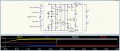
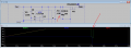
Here's an updated version of my suggested circuit with mods which, with the component values shown, should allow it to work even with ripple as high as ~10% on a 12V supply.
The MOSFET models in the sim are arbitrary ones from the LTS library, but in the real world would be chosen according to the power supply voltage, load current, availability, and price.
Parameters Volts and rip are the input supply voltage and the ripple factor.
1728729931832.png
 

Attachments

Thread Starter

yef smith

Joined Aug 2, 2020
1,472
Hello Alec,I have removed the Rload resistors and connected the sequencer circuit which is the real load.
I put the source you used in the original circuit (without noise,because i want to simulate noise using noise source)
The sequencer output is great.
However as you can see the In+ startup ramp crosses entirely to the out+ .
What could cause that in the Pulse circuit? How can I make it function properly?
Thanks.
LTSPICE file is attached.
1728740633390.png1728740582251.png

Sequencer output:
1728740957645.png
 

Attachments

Alec_t

Joined Sep 17, 2013
15,132
However as you can see the In+ startup ramp crosses entirely to the out+ .
What could cause that in the Pulse circuit?
You are saving data from 2.08 seconds onwards, whereas the In+ voltage ramps up over 1 second so is not seen.

Edit:
Because of the capacitor on M1 gate, M1 switches on relatively slowly. Only when it is nearly fully on does M2 switch on. There is thus a slight delay between Out- going low and Out+ going high. This delay is reflected in the non-overlapping of the Vdd_out, Vg1 and Vg2 edges.
 
Last edited:

Thread Starter

yef smith

Joined Aug 2, 2020
1,472
Hello Alec,The sequencer solves this issue totally.
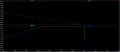
As you can see below, I dont have a ramp on the outputs.
But on the output of the stabilizer pulse circuit we do have this ramp on the output,although in the Bjt version we didnt have such problem.
Is there a way you could recomend to remove this ramp from OUT+?
in this circuit OUT+ almost copies IN+.
Is there a way to correct that?
Thanks.
.1728748389683.png
 

sparky 1

Joined Nov 3, 2018
1,218
In an analog scenario 2 capacitors charge according to the RC time constant formula.
If the resistors values are slightly different the charge time will be slightly different.
The delay time is chosen by the resistor value. The RC timing circuit makes sequence timing possible.
A washing machine in the past had a timing controller driven by a motor with mechanical switching.

In a capacitor charge circuit, an led shows when the capacitor is fully charged. The led can be replaced with a transistor
that acts as a switch to activate a sequence.
In the field of PLC (programmable logic control) current mode is usually preferred because of distance and noise.
A micro controller can be used for some PLC applications. There are bad designs and faulty products, cheap garbage.
The industrial PLC controllers are more expensive however the designs are usually reliable.
 
Last edited:

Thread Starter

yef smith

Joined Aug 2, 2020
1,472
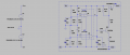
Hello Alec, I see the situation that M2 PMOS outputs the signal almost from the start.
So it needs to open the same as M1.I tried to add a capacitor as shown bellow but it created adelay in a different place shown below
How do you reccomend tomake M2 to be closed when there is a ramp in In+?
Thanks.

"Because of the capacitor on M1 gate, M1 switches on relatively slowly. Only when it is nearly fully on does M2 switch on. There is thus a slight delay between Out- going low and Out+ going high. This delay is reflected in the non-overlapping of the Vdd_out, Vg1 and Vg2 edges."

1728757879145.png1728757537837.png
1728758943628.png
 

Alec_t

Joined Sep 17, 2013
15,132
How do you reccomend tomake M2 to be closed when there is a ramp in In+?
I've found a cure for the glitch. Connect a resistor between Out+ and ground. Any value up to 10meg seems to work, so I suspect drain-gate capacitance of M2 may be the culprit.

Edit:
I think the underlying cause of the glitch was that both Out+ and Out- need a well-defined path to ground while In+ and In- are ramping up.
 
Last edited:

Thread Starter

yef smith

Joined Aug 2, 2020
1,472
Hello Alec,Yes it works.In real PCB i should put the 10MEG resistor too?
how the gate drain capacitance caused the M2 to be open all the time?

why adding resistors solves it?
Thanks.
 
Last edited:

Alec_t

Joined Sep 17, 2013
15,132
how the gate drain capacitance caused the M2 to be open all the time?
I no longer think that was the culprit. Did you see the edit in post #38?
In a real pcb there may already be a deliberate or leakage path to ground, obviating the need for that extra resistor.

Edit:
Further analysis indicates that when M2 is off there is slight leakage across it (<1 nanoAmp), source to drain. In the absence of a well-defined current sink path from Out+ to ground while In+ is ramping up, the voltage at the drain (Out+) follows the source voltage (In+).
 
Last edited:
Top