converting power supply signal into pulse signal

Thread Starter

yef smith

Joined Aug 2, 2020
1,472
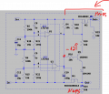
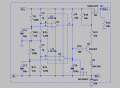
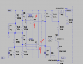
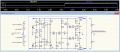
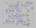
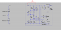
Hello Alec, I am trying to understand the first part of the circuit shown below.
We have an input positive and negative pulses which dont happen in the same time and they have different slopes.
The positive leg of each comparator connected to 10uF 15Kohm 100Kohm.
The negative leg of each comparator is connected to 270K and 1uF.
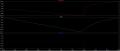
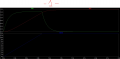
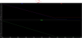
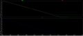
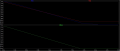
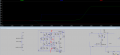
There are photo of the signals after the RC network going into the input.
I know
What did you tried to achieve for the input of the comparators?
Thanks.
1728992835312.png


negative leg input to the comparator:

1728993405280.png

positive leg input to the comparator:

1728993546493.png
 

Alec_t

Joined Sep 17, 2013
15,132
Using you component numbering:
C11,R5 form an integrator, so the voltage at a lags behind the rising In+ voltage.
C8,R21 form a differentiator, so the voltage at b rises quickly as In+ rises.
Therefore b is always more positive than a while In+ is rising.
Therefore U1 output pulls low while In+ is rising.
When In+ stops rising b drops to ground, but a remains a bit above ground by virtue of the voltage drop across R20. Therefore U1 output no longer pulls low.

A similar scenario applies to U2 and its input circuitry.
Only when U1 and U2 have both stopped pulling low can node e get pulled up by R4.
 

Thread Starter

yef smith

Joined Aug 2, 2020
1,472
Hello, node "e" is rising after the pulses stabilize.
There are PMOS and NMOS which need to be open simultaniosly.
What is the logic in using NPN with a diode to open these mosfets?
Also why M1 has 100uF capacitor at the gate while M2 has only resistors?
Thanks.
1729023827667.png
 

Alec_t

Joined Sep 17, 2013
15,132
What is the logic in using NPN with a diode to open these mosfets?
The PMOS needs its gate pulled down to turn it on, so an inverter (the npn) is needed because e goes high.
The diode D2 prevents reverse voltage which would otherwise appear across the base-emitter junction from causing junction breakdown. If you plot the voltage between nodes e and Out- you will see the reverse voltage.
Also why M1 has 100uF capacitor at the gate while M2 has only resistors?
C1 prevents supply rail noise from causing spurious switching of M1 and consequently M2.
 

Thread Starter

yef smith

Joined Aug 2, 2020
1,472
Hello Alec,Yes npn needs Vbe=0.7 so if emitter voltage will rise then NPN will be closed.
few questions:
1.Ve and V(e,Out) plot is shown below where is the dengerous zone where the NPN will be closed?
2.what is the intuition you desided by to use 100uF?
What tests you did to see that 100uF is enough?
Did you do noise simulations you could share so i could see the intuition?
3.how did you desided the values for the integrator and differentiator?
4.You said i should choose PMOS and NMOS, I chose them by maximum rating.
I chose SI4467DY PMOS, and Si4364DY NMOS.
the data sheet of them says they can handle current.
5.do you reccomend to use a certain type of capacitors ? should I electrolithic type (not ceramic)?
Thanks.
1729087523768.png

1729088609669.png
 
Last edited:

Alec_t

Joined Sep 17, 2013
15,132
where is the dengerous zone where the NPN will be closed?
When e rises enough to turn on M1 sufficiently to lower Out- such that v(be) is ~0.65V. This zone is a bit vague because no two NMOS or PMOS devices are identical, their turn-on points are not sharply defined, and the turn-on points of the NPN and PMOS are similarly gradual rather than abrupt.
what is the intuition you desided by to use 100uF?
Trial and error, dependent on rail ripple magnitude.
Did you do noise simulations you could share so i could see the intuition?
I didn't.
.how did you desided the values for the integrator and differentiator?
Trial and error.
do you reccomend to use a certain type of capacitors ?
If >> 1uF use electrolytic. If <= ~1uF use ceramic or polyester. Not critical in this circuit.
 
Last edited:

Thread Starter

yef smith

Joined Aug 2, 2020
1,472
Hello Alec, I was given a remark about this design that a slow rising voltage (filtered by C10) to two output stages with different threshold and control characteristic. Even I manage to adjust the thresholds, voltage rise time of + and - output will be different and load dependend though.

Is that logical to you ?
because the outputs of the comparatorsis slow risingthe output will be dependant on the load?
I cant see how these two link together?
Thanks.
 

Alec_t

Joined Sep 17, 2013
15,132
The ability of the comparators to respond as intended to increasingly positive and increasingly negative voltages wll be affected by the rates of change of those voltages, possibly needing experimental adjustments of the associated RC time constants for much slower ramps than you show.
Comparator response will not be affected by the MOSFET loads, but because M1 is not switched on abruptly its load response might be affected by that.
If that were a concern, then a buffer stage could be introduced between the node e and the MOSFET-enabling circuitry, to ensure faster turn-on of both MOSFETs.
 

Thread Starter

yef smith

Joined Aug 2, 2020
1,472
Hello Alec, regarding the first part I think the simulation said that power supply can handle the ramps.
regarding the second part :
Why if we increase the gate of the M1 gradually then its become dependant?
The condition for opening NMOS is Vgs>Vt why it matters how fast Vg is rising?
the load of the NMOS is the drain.


first part:
The ability of the comparators to respond as intended to increasingly positive and increasingly negative voltages will be affected by the rates of change of those voltages, possibly needing experimental adjustments of the associated RC time constants for much slower ramps than you show."

second part:
but because M1 is not switched on abruptly its load response might be affected by that.
If that were a concern,
 

Alec_t

Joined Sep 17, 2013
15,132
The condition for opening NMOS is Vgs>Vt
It depends what you mean by 'opening'. When Vgs=Vt the FET is only just beginning to conduct a few microAmps. To turn a standard FET fully on usually needs a Vgs of about 10V. Look at the datasheet for a typical FET and note the graph of drain current as a function of Vgs.
the load of the NMOS is the drain.
The load is the current-consumer connected to the drain.
 

Thread Starter

yef smith

Joined Aug 2, 2020
1,472
Hello Alec, I am try to improve the circuit so U1 and U2 will work as you said.
Regarding U2 you said that as U11 voltage on nodes D is larger then voltage on node C while In+ is rising.
Is there an intuition how to improve the situin so node D will be larger then node C only when In+ is rising?
Thanks.

LTspice file is attached.
1729424635032.png
 

Attachments

Alec_t

Joined Sep 17, 2013
15,132
Is there an intuition how to improve the situin so node D will be larger then node C only when In+ is rising?
Why do you want that to happen? U2 handles the negative supply rail. My design keeps d>c only while In- is ramping down.
Your value for R15 is much too small a fraction of R6 to have any significant effect and could cause problems if there is ripple on the supply rails.
 

Thread Starter

yef smith

Joined Aug 2, 2020
1,472
Hello Alec ,Yes I understand, so photo 1 is showing clearly B>A while In+ is rising.
I clearly got to the situation you described(with my own little tuning)
but if when i look at the original RC situation for U2 ,C D nodes:
C and D nodes are very close to each other as shown in photo 2.
Is there a way to make D>C more clearly while Vin- is decreasing?
Thanks.
1729428889592.png
1729429197030.png
1729429306514.png
1729430874871.png
 

Attachments

Thread Starter

yef smith

Joined Aug 2, 2020
1,472
Hello Alec, I have started to build a PCB from the simulation,three questions:
1.I am used to put decoupling capacitors of 10uF,1uF,0.1uF near each power supply rails of the
given the fact that our supply to U1 and U2 is not contant .
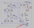
do you recommend to put 10u 1u 0.1u capacitors near each power rail of U1 and U2 as shown bellow in the red arrow?
In the LTspice simulation i cant see something getting worse.
2.You said I should use electrolytic capacitors for values larger then 1uF.
they have very complex footprint.
can I use tantalum capacitors instead shown below?
https://www.digikey.com/en/products/detail/kyocera-avx/TAJC226K025RNJ/563817

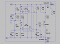
3.C10 is very important and I sawas shown bellow when I put C10 to be 20uF instead of 100uF then +12 and -12 pulses become closer, but on the other hand you said C10 is important to get the node "e" stable from noise.
How can i see in the lab the effect of C10 to make node "e" stable?
so i'll know to increase the C10 value if its capacitance is not enough?
Thanks.
1730013005337.png

1730015821304.png
1730016260087.png
1730016381315.png
 

Alec_t

Joined Sep 17, 2013
15,132
As you now seem keen to have Out+ and Out- enabled as closely as possible to simultaneously you might want to consider this (albeit slightly more complex) circuit modification:
1730020404795.png
In this circuit Q1 and Q2 form a latch. Q3 and Q4 provide low-impedance drives for the MOSFET gates.
As for using tantalum capacitors, I've no experience with them but I do understand there can be problems if they're not used correctly.
 

Attachments

Thread Starter

yef smith

Joined Aug 2, 2020
1,472
Hello Alec,Thank you very much, I want to produce a PCB from the previos best version, because it works great too.
few PCB questions:
1.do you reccomend to put ceramic decoupling capacitor of 10uF 1uF 0.1uF as i put in the photo below of U1 U2?
2.You recommended to use electrolytic capacitors for large values larger then 1uF
here is a capacitor I found at mouser.
Is this the right type you reccomend to use?
Thanks.
https://www.mouser.com/ProductDetai...=sGAEpiMZZMvwFf0viD3Y3Yd5qvTVv7orAn35MfmoRWU=
1730028051633.png
 

Thread Starter

yef smith

Joined Aug 2, 2020
1,472
Hello Alec, decoupling capacitors makes the voltage power rail stable.
But in our case Our power rail is not stable because the power supply is not stable.
So you say its ok to use ceramic capacitors near IC power rail?
I dont understand how the shape of the capacitor has an influence?
Thanks.
 
Top