Connectors: Ground edges? Mechanical post-hole size? Weird through-hole "pin"?

Thread Starter

danielmhartmann

Joined Oct 19, 2020
3
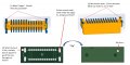
Hello. I'm an inexperienced circuit designer and I've never designed a PCB with connector-headers until now. I'm using Harting 26-pin surface-mount connector/header 15110262601000 and I downloaded the footprint and CAD from Digikey and imported them into KiCAD for my PCB layout. I have three questions for folks who've worked with connectors like this. (1) The connector has metal edges and the footprint appears to provide pads to which those edges may be soldered. Should I do that, aand should I connect those pads to ground? (2) There are two mechanical posts on the connector, 1.5mm in diameter. What size hole should I use in the circuit board to ensure good fit? Should it be slightly-oversized / undersized, or line-to-line? (3) There's a strange feature in the footprint that I don't understand; it looks like a metal pin, offset-slightly from the footprint, and it goes all the way through the board. (So if you flip the two layer board, you see the pin on both sides). Any idea what this is, or what I should do with it? Thank you in advance! Dan
 

Attachments

ronsimpson

Joined Oct 7, 2019
4,660
(1) It probably does not matter on this connector. On many, these might be connected to the shield of the cable and should go to ground. On many connectors these make contact first and are used for static protection. I would take them to ground even if they are not electrically connected.
(2) Does the CAD footprint call out hole size? You might have to do a gerber print to see what happens for the hole.
(3) Indicates pin1.
 

Thread Starter

danielmhartmann

Joined Oct 19, 2020
3
Awesome. Thank you, Ronsimpson. I'll ground the edges just like you suggest, and do some test prints for the hole size. Regarding question 3: the footprint seems to have a different mark that (also?) indicates pin1. I'm attaching a screenshot from KiCAD. The mark that I thought indicated pin1 is right on top of the pin, whereas the mark that puzzles me is off to the side, and over near one the "X4" edge. Perhaps they both are meant to indicate pin1? It's weird to me that one of them is off to the side, and that it appears to go all the way through the board, so it's visible on both sides.Pin1-question-from-KiCAD.JPG
 

Thread Starter

danielmhartmann

Joined Oct 19, 2020
3
Yes! You are right. It's silkscreen on both sides. Thank you! Still not sure why it's there, but at least I know it's nothing electrical. Really appreciate your quick replies.
 

ronsimpson

Joined Oct 7, 2019
4,660
I often modify footprints. It is a little dangerous, not modifying can also get you in trouble. LOL
It often print out a footprint, or board at 1:1 scale and place the parts on a paper board. I have found cases where someone made a part at 2:1 off scale.
 

MisterBill2

Joined Jan 23, 2018
27,292
That item that appears to go thru the board CERTAINLY MUST go thru the PCB. THAT is how to assure that the connector is placed correctly, and how it stays correctly positioned for wave or reflow soldering. That hole in the PCB should be a "close fit". The CAD file that you got should specify the diameter. If you are lucky.
 
Top