[Confused] Calculation for Transistor

Thread Starter

sdas86

Joined Mar 18, 2015
26
Dear all friends,
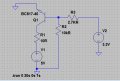
I am confused. When I saw this circuit, I don't know how to calculate.
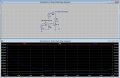
Attached is the circuit. I tried using LTSpcice to simulate but the values are not quite right. I am not sure.

Hope to get some help here. Can teach me how to calculate - Vr3, Vr2, Vr1?

Thanks.

Regards,
William
 

Attachments

AnalogKid

Joined Aug 1, 2013
10,986
You can calculate your three values with Ohm's Law if you have two more pieces of information. First, you need the base-emitter voltage of the transistor when it is its linear active region. Also, you need a graph of the gain of the transistor vs. its collector current. The calculations would be easier if R1 were larger.

ak
 

MikeML

Joined Oct 2, 2009
5,444
First, I redrew your circuit to match the way that it is usually depicted. To answer your questions about node voltages and component currents, you need to label some of the nodes. Then use the DC ANALYSIS built into LTSpice to display the voltages and currents. To do this, use a .DC simulation directive instead of .TRAN, which is for time-domain (transient) solutions where you want to see nodes change vs time.

Look at this:

209dc.gif

You can see immediately that Q1 does not have enough base current to cause it to switch on fully. Note V(c), I(R1) or Ic(Q1), and Ib(Q1).

Now, assuming that you are really trying to get this transistor to switch a 10Ω load, you would have to drive the base of Q1 with a much higher base current. To do that, you could make R3 smaller, so let us ask LTSpice to show us what value of R3 would cause Q1 to fully turn on (saturate) by making V(c) as low as possible. I reconfigure the LTSpice simulation to do multiple .DC solutions while varying R3 and cause it to plot the results.

209sw.gif

Note the following:

LTSpice automatically plots whatever node voltages or currents that you select vs R3 (the independent variable of the simulation). It does repeated .DC solutions because I told it to do so with the .step PARAM statement, which steps R3 from 500Ω to 5000Ω in steps of 20Ω. Curly braces { } are used to pass the parameter to change the value of R3 for each new simulation.

Note that for values of R3 less than about 800Ω turns on Q1 about as well as it can be. That causes V(c) green trace to get low enough to where Q1 is approaching saturation. I plot the current through R3 I(R3) red trace to see how much current the source V2 would have to supply in order to saturate Q1. Note that it takes more than 2.8mA to do that...

Finally, to show off another feature of LTSpice, I plot the power dissipation in Q1 (blue trace). Note that with your original value of R3=2700Ω, Q1 would overheat because this little transistor is dissipating ~0.62W. If the goal is to switch the 10Ω load on-off, then you must use a higher base current to get through the point of highest dissipation quickly...

Note how LTSpice keeps track of multiple plots on the same x-axis, keeping the units separate. Here I am plotting voltage, current and power...
 

crutschow

Joined Mar 14, 2008
34,283
Note that Mike's simulation will show you the required base resistor to fully turn on the transistor for a transistor with nominal gain, not one with minimum gain (transistor gain has a wide tolerance from unit to unit).

The usual value of gain used to insure full saturation of and BJT transistor is 10, so the base current should be at least 1/10th of the collector current, or 50ma for the test circuit collector current of 0.5A.

Also note that you should not operate a transistor or other semiconductor at its rated voltage or current values. Always derate at least 30-50% for best reliability.
 

Thread Starter

sdas86

Joined Mar 18, 2015
26
Some numbers are missing.
Vce(on)?
Vbe(on)?
You can calculate your three values with Ohm's Law if you have two more pieces of information. First, you need the base-emitter voltage of the transistor when it is its linear active region. Also, you need a graph of the gain of the transistor vs. its collector current. The calculations would be easier if R1 were larger.

ak
Dear shteii01 and AnalogKid,
The transistor I am using is http://www.farnell.com/datasheets/1842041.pdf. From the datasheet, I do not see the Vce(on) an Vbe(on). Am I reading it wrongly? Please advice me. Thanks guys/girls. :)


First, I redrew your circuit to match the way that it is usually depicted. To answer your questions about node voltages and component currents, you need to label some of the nodes. Then use the DC ANALYSIS built into LTSpice to display the voltages and currents. To do this, use a .DC simulation directive instead of .TRAN, which is for time-domain (transient) solutions where you want to see nodes change vs time.

Look at this:

View attachment 85648

You can see immediately that Q1 does not have enough base current to cause it to switch on fully. Note V(c), I(R1) or Ic(Q1), and Ib(Q1).

Now, assuming that you are really trying to get this transistor to switch a 10Ω load, you would have to drive the base of Q1 with a much higher base current. To do that, you could make R3 smaller, so let us ask LTSpice to show us what value of R3 would cause Q1 to fully turn on (saturate) by making V(c) as low as possible. I reconfigure the LTSpice simulation to do multiple .DC solutions while varying R3 and cause it to plot the results.

View attachment 85650

Note the following:

LTSpice automatically plots whatever node voltages or currents that you select vs R3 (the independent variable of the simulation). It does repeated .DC solutions because I told it to do so with the .step PARAM statement, which steps R3 from 500Ω to 5000Ω in steps of 20Ω. Curly braces { } are used to pass the parameter to change the value of R3 for each new simulation.

Note that for values of R3 less than about 800Ω turns on Q1 about as well as it can be. That causes V(c) green trace to get low enough to where Q1 is approaching saturation. I plot the current through R3 I(R3) red trace to see how much current the source V2 would have to supply in order to saturate Q1. Note that it takes more than 2.8mA to do that...

Finally, to show off another feature of LTSpice, I plot the power dissipation in Q1 (blue trace). Note that with your original value of R3=2700Ω, Q1 would overheat because this little transistor is dissipating ~0.62W. If the goal is to switch the 10Ω load on-off, then you must use a higher base current to get through the point of highest dissipation quickly...

Note how LTSpice keeps track of multiple plots on the same x-axis, keeping the units separate. Here I am plotting voltage, current and power...
Dear Mike,
I really thank you for this great help. I have to admit my LTSpice simulation skill is truly newbie level. By the way, the transistor I am using for the hardware is http://www.farnell.com/datasheets/1842041.pdf. Is this simulation work the same if this transistor(the datasheet of the url )is used?


Note that Mike's simulation will show you the required base resistor to fully turn on the transistor for a transistor with nominal gain, not one with minimum gain (transistor gain has a wide tolerance from unit to unit).

The usual value of gain used to insure full saturation of and BJT transistor is 10, so the base current should be at least 1/10th of the collector current, or 50ma for the test circuit collector current of 0.5A.

Also note that you should not operate a transistor or other semiconductor at its rated voltage or current values. Always derate at least 30-50% for best reliability.
Dear crutschow,
I saw from the datasheet as attached "Gain.jpg". It shows the gain BC817-16 Min-Max: 100-250 and BC817-40 Min-Max: 250-600. For this simulation, my LTSpice does not have BC817-16, so I use BC817-40, what should I do?

From Mike's simulation, you mentioned that it is nominal gain. Nominal gain means the gain in between 250-600 for BC817-40 Min-Max: 250-600?

Sorry, I am very confused.

Thanks a lot for all the help here! Thumbs up!
 

Attachments

crutschow

Joined Mar 14, 2008
34,283
The gain shown in the data sheet is for operation in the linear region as an amplifier, not as a switch.
When used as a switch you should use a gain of 10 for reliable operation.
 

MikeML

Joined Oct 2, 2009
5,444
The gain shown in the data sheet is for operation in the linear region as an amplifier, not as a switch.
When used as a switch you should use a gain of 10 for reliable operation.
Maybe if you are building 100,000 identical widgets on a production line and have to play the statistics game that 99.9% of the devices work with minimal testing. On the production line, there is a small probability that you will get a transistor in a shipment of thousands of transistors that will have the worst case gain.

If you are a hobbyist building a one-of device, then you do not have to play this game. Instead of designing for the third sigma in the spread, design for the middle sigma.

Using Ic/Ib = 10, for this circuit, the base current would have to be ~500mA/10 = 50mA. It is likely that the base current is being supplied by a 3.3V CMOS logic signal which will not source 50mA, more like 20mA.

So would 20mA turn on a BC817-16L sufficiently to make its Vce less than 1V? I think it would... but, this transistor is so marginal for this application that I would hesitate to use it.

Note that it is being operated at its do-not-exceed maximum collector current of 500mA. In addition, the max power dissipation allowed is only 225mW when soldered to ~1 square inch of FR5 PCB material, provided that the ambient temperature is 25degC. The power dissipation must be reduced by 1.8mW per degC over 25degC.

At an ambient temp of 45 degC, the allowed dissipation is 225-1.8*20 = 189mW, so if the collector current is 500mA, the Vce must be less than 189mW/500mA = 0.378V.

This is a very marginal design that isn't going to be fixed by adding to the transistor's dissipation by pouring 50mA*1.2V= 60mW into its base-emitter junction.
 
Last edited:

Thread Starter

sdas86

Joined Mar 18, 2015
26
The gain shown in the data sheet is for operation in the linear region as an amplifier, not as a switch.
When used as a switch you should use a gain of 10 for reliable operation.
Dear Mike and crutcshow,
How do we know what gain we are using based on the simulation circuit? Is there any calculation to calculate?
Thanks.


Strange. The datasheet says that Vbe(on) is 1.2 volts.

View attachment 85666

I think the Vce(on) is the 1 volt. Somebody double check me please.
Dear shteii01,
The datasheet Vbe(on) is 1.2V max. From my circuit (attached), the cyan color line is the Vbe at point "b" which is 0.9V. So, this means my transistor is not turning on?

Thanks!
 

Attachments

Thread Starter

sdas86

Joined Mar 18, 2015
26
Maybe if you are building 100,000 identical widgets on a production line and have to play the statistics game that 99.9% of the devices work with minimal testing. On the production line, there is a small probability that you will get a transistor in a shipment of thousands of transistors that will have the worst case gain.

If you are a hobbyist building a one-of device, then you do not have to play this game. Instead of designing for the third sigma in the spread, design for the middle sigma.

Using Ic/Ib = 10, for this circuit, the base current would have to be ~500mA/10 = 50mA. It is likely that the base current is being supplied by a 3.3V CMOS logic signal which will not source 50mA, more like 20mA.

So would 20mA turn on a BC817-16L sufficiently to make its Vce less than 1V? I think it would... but, this transistor is so marginal for this application that I would hesitate to use it.

Note that it is being operated at its do-not-exceed maximum collector current of 500mA. In addition, the max power dissipation allowed is only 225mW when soldered to ~1 square inch of FR5 PCB material, provided that the ambient temperature is 25degC. The power dissipation must be reduced by 1.8mW per degC over 25degC.

At an ambient temp of 45 degC, the allowed dissipation is 225-1.8*20 = 189mW, so if the collector current is 500mA, the Vce must be less than 189mW/500mA = 0.378V.

This is a very marginal design that isn't going to be fixed by adding to the transistor's dissipation by pouring 50mA*1.2V= 60mW into its base-emitter junction.
Dear Mike,
Is it for normal design, Ib = Ic/10? For our simulation, if we are using 800Ohm resistor at R3, the current will be 3.2mA. Is this sufficient to switch on the transistor? I would like to ask which part of the datasheet shows this Ib switch on current. I can't find the information for Ib switch on current on datasheet.

Thanks.
 

crutschow

Joined Mar 14, 2008
34,283
...................
I would like to ask which part of the datasheet shows this Ib switch on current. I can't find the information for Ib switch on current on datasheet.
If you look at the portion of data sheet shown in post #8, you will see that the collector-emitter saturation voltage (where the transistor is fully on) is specified with a base current of 50mA for a collector current of 500mA (gain of 10).
 

Thread Starter

sdas86

Joined Mar 18, 2015
26
If you look at the portion of data sheet shown in post #8, you will see that the collector-emitter saturation voltage (where the transistor is fully on) is specified with a base current of 50mA for a collector current of 500mA (gain of 10).
Thanks for the explanation. Now I understand. :)
 

MikeML

Joined Oct 2, 2009
5,444
If you look at the portion of data sheet shown in post #8, you will see that the collector-emitter saturation voltage (where the transistor is fully on) is specified with a base current of 50mA for a collector current of 500mA (gain of 10).
But that does not mean that the base has to be driven with 50mA to switch 500mA. It just says the the transistor maker guarantees that any transistor that is shipped will have a saturation voltage of 0.7V or less if Ic=500mA and Ib=500mA.

sdas86 never addressed the unsuitability of this transistor for this application (no matter how hard the base is driven) I raised in post#9, above.
 

crutschow

Joined Mar 14, 2008
34,283
But that does not mean that the base has to be driven with 50mA to switch 500mA. It just says the the transistor maker guarantees that any transistor that is shipped will have a saturation voltage of 0.7V or less if Ic=500mA and Ib=500mA.
................
That's true. You could likely use some higher value of forced gain, such as 20, and most transistors would still saturate.
But using the simulation of a transistor with nominal gain to determine the base current required for saturation will likely give a circuit design that will not fully saturate for many transistors from a random lot.
If you changed the simulation model to have minimum gain, then the simulation would be more accurate in giving the base current required for saturation for most (and perhaps all) transistors in a lot.
 

Thread Starter

sdas86

Joined Mar 18, 2015
26
But that does not mean that the base has to be driven with 50mA to switch 500mA. It just says the the transistor maker guarantees that any transistor that is shipped will have a saturation voltage of 0.7V or less if Ic=500mA and Ib=500mA.

sdas86 never addressed the unsuitability of this transistor for this application (no matter how hard the base is driven) I raised in post#9, above.
Dear Mike,
Sorry, I missed that post #9. Now, I read back and understand.

Thanks for all the help. You guys are great! Thumbs up!;)
 

Thread Starter

sdas86

Joined Mar 18, 2015
26
That's true. You could likely use some higher value of forced gain, such as 20, and most transistors would still saturate.
But using the simulation of a transistor with nominal gain to determine the base current required for saturation will likely give a circuit design that will not fully saturate for many transistors from a random lot.
If you changed the simulation model to have minimum gain, then the simulation would be more accurate in giving the base current required for saturation for most (and perhaps all) transistors in a lot.
But that does not mean that the base has to be driven with 50mA to switch 500mA. It just says the the transistor maker guarantees that any transistor that is shipped will have a saturation voltage of 0.7V or less if Ic=500mA and Ib=500mA.

sdas86 never addressed the unsuitability of this transistor for this application (no matter how hard the base is driven) I raised in post#9, above.
Dear Mike and crutschow,
I found out that the Digital I/O output from my device is maximum 20mA.
One thing I do not really understand. From our simulation circuit and the graph, if we are using 500Ohm resistor at R3, does this mean that the maximum current going into the base will be 4.8mA?
From the graph, it shows that 500 ohm and 4.8mA for I(R3).

If 4.8mA is the maximum, then the chances of this transistor on or off is hard to predict?

Thanks.
 

MikeML

Joined Oct 2, 2009
5,444
That's true. You could likely use some higher value of forced gain, such as 20, and most transistors would still saturate.
But using the simulation of a transistor with nominal gain to determine the base current required for saturation will likely give a circuit design that will not fully saturate for many transistors from a random lot.
If you changed the simulation model to have minimum gain, then the simulation would be more accurate in giving the base current required for saturation for most (and perhaps all) transistors in a lot.
I take the required base current determined from the nominal gain, and adjust it by the ratio of nominal gain/min gain. For the BC417-40, for example, I would say that a base current as determined by simulation of 3mA* (nominal gain)/(min gain) = 3mA * 400/250 ~= 5mA would be good enough...

As a data point, I have done this many times, an never had a problem where the transistor "doesn't turn on". Maybe my way the Vcesat is a 100mV higher than could be achieved by pouring in more base current, but it has never failed to work. Now usually, when I do this, I am not trying to switch 500mA with a transistor whose absolute maximum allowed Ic is 500mA..., and I dont care if the transistor dissipates 50 or 100mW more than it would with more base current.
 

Thread Starter

sdas86

Joined Mar 18, 2015
26
Thanks for the explanation. :)

I would like to ask can I control a relay using this circuit? The relay has 60 ohm resistance (as shown in image attached).
The curve has changed from the previous simulation after adding the 60ohm resistance at Collector.
 

Attachments

Top