Why have U1A oscillator at all? In other words, what is the relationship between the inputs of U1C? I've done some gold panning, maybe I'll make myself a detector and become RICH.
What I'd like are comments on the viability of the connection from the output terminal of gate U1C to an input terminal of gate U1D, and the configuration of gate U1D as a low pass filter with a cut-off frequency of 10kHz.
My simulation shows oscillation of the last gate due to feedback, similar to the high-frequency oscillation of the oscillator.
For that you can add an op amp or audio amp, such as AK suggested, to provide the 10kHz filter rolloff, and buffer to the headphones.
There are two oscillators, operating about 1kHz apart.
One of the oscillators has the tank circuit in the detector head which changes frequency slightly when metal is near the head.
This small change causes a change in the 1kHz difference frequency that is detected and sent to headphones, where the change in frequency is readily detected by the ear.
For example, a 0.1% change in the 160kHz oscillator frequency of 160Hz results in a 16% change in the 1kHz difference frequency.
There are two oscillators, operating about 1kHz apart.
One of the oscillators has the tank circuit in the detector head which changes frequency slightly when metal is near the head.
This small change causes a change in the 1kHz difference frequency that is detected and sent to headphones, where the change in frequency is readily detected by the ear.
For example, a 0.1% change in the 160kHz oscillator frequency of 160Hz results in a 16% change in the 1kHz difference frequency.
Aside from the many previous comments there is the variability of components, including that IC, which they do vary with temperature and production lot and manufacturer. And certainly wiring technique can make a large difference.
Beyond those variables there is also the "Q" factor of that tuned circuit, with the coil resistance having a real effect. So it is not a bad design, but rather a whole lot of variables that have an unknown effect on the frequency. Get an IC from the same production run as the one in the original and the results may be closer.
And for oscillators with the same circuit, that part is a good design. consider that the 1 khz difference is much less than 1% of the oscillator frequency. So if 5% tolerance parts were used it is very likely that adjusting will be needed to bring the oscillators that close to the same frequency. Component values of 5% tolerence parts are never within 1% of the marked value because the ones much closer are sold as 1% parts at a much higher price.
Their frequencies are identical only with perfect components.
In practice one of the oscillators is tweaked by one of its capacitor values so it is abut 1kHz different from the other.
That circuit seems to be for a very low budget metal detector , optimized for minimum cost to produce. In fact it is difficult to imagine a circuit much simpler that would actually work very well. It can also be adjusted so that the two frequencies match very closely, and then it would be even more sensitive, but less stable.
An oscillator using a gate like that is a fairly high impedance circuit and thus it will be greatly affected by the mechanical arrangement of the parts. So if the circuit is built on a breadboard, or even a prototype board, it is not very likely to perform as anticipated. It was probably traced off of an actual product, and so the parts values may have been misread, as well.
I had not considered an XOR as a frequency mixer, but certainly it could be. I had an article about a digital frequency readout for a receiver that mixed the local oscilatir frequency with the IF converter and the BFO to display the signal frequency, it used and gates and a JK flipflop as a digital mixer. Certainly an XOR would be simpler. I wonder if it would work.
If I understand correctly the circuit is functioning as a digital amplifier where the difference between the two input frequencies is proportional to the output mixed frequency ignoring filtering. It would be otherwise difficult to detect the very small field interactions when passing over a mineral.
If I'm on the right track, what happens when the signals are out of phase which I would assume is the case in this situation?
Out of phase is not a condition since the signals are not the same frequency. As the frequencies become close the result is more like a PWM sinal varying at the rate equal to the difference of the frequencies.
Well I was able to get the two gates oscillating each at frequency equal to about 160 kHz and with close to a 1 kHz difference of frequency. This occurred where a first inductor is a bobbin coil, and the second inductor was air core bank wound 5 mH, 4 mH, and 1 mH coils connected in series. This arrangement was very stable.
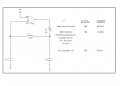
However, when i substituted a coil of 6 inch diameter of the needed inductance (10 mH) for the three bank wound coils connected in series, this resulted in very unstable oscillation of the gate that it is connected to. As shown in the below circuit diagram, for the 6 inch diameter search coil. decreasing capacitance of C1 = C2 from 150pf to 100 pf results in increasing the frequency of oscillation by more than 20 times. Also I found it impossible to get the gate that the search coil was connected to to oscillate at around 160 Hz by adjusting C1 = C2.
Can anyone explain why the 6 inch dia. coil results in a jump from oscillation in the kHz to MHz range when making a relatively small change to capacitance of C1 = C2? If I were to make the diameter of the search coil 4 inches diameter, would that allow for stable oscillation at around 160 kHz (according to the original design of the metal detector)?
I'm incorporating Crutschow's advice to eliminate capacitance in parallel with the inductors in my revised design of the metal detector.
Can anyone explain why the 6 inch dia. coil results in a jump from oscillation in the kHz to MHz range when making a relatively small change to capacitance of C1 = C2
There may be enough parasitic parallel coil capacitance to cause the same high frequency oscillations that you saw with the discrete added capacitor.
Perhaps a small inductor in series with the coil would prevent that.
There is certainly enough capacitance in that coil to affect the resonant frequency. And a coil wound with #18wire will have a lot more wire surface capacitance. and scramble wound affects it as well. So the unknown capacitances between different parts of the circuits each add their own effect.
My LTspice simulation also showed a several MHz oscillation.
When I removed C1, then the oscillation went to 158.7KHz, very near the 159.2KHz calculated for the LC tank values used below (10mH in parallel with 100pF series equivalent).
I expect C1 was causing the high-frequency oscillation from it providing a path for positive feedback caused by the high-frequency phase-shift of the gate.
C1 has a low impedance at a couple MHz so the feedback signal is coupled directly through it.
Since C2 and C3 in series through the ground connection now provide the tank parallel capacitance, I don't see a need for C1.
Crutschow, where did you get the 2 input exclusive or gate for your simulation? In the version of LTspice that I have, the only gates that are available have multiple inputs, and I believe that they are named behavioral gates, whatever that is. I would like to look at different configurations of the XOR gate as an oscillator, and that would go much more quickly simulating than with hardware.
I'm getting more involved with the metal detector than I wanted to, but I guess that's the way it goes.
Thank you if you can point me to a source of components, or did you create that 2 input XOR gate yourself?
Crutschow, where did you get the 2 input exclusive or gate for your simulation? In the version of LTspice that I have, the only gates that are available have multiple inputs, and I believe that they are named behavioral gates, whatever that is. I would like to look at different configurations of the XOR gate as an oscillator, and that would go much more quickly simulating than with hardware.
I'm getting more involved with the metal detector than I wanted to, but I guess that's the way it goes.
Thank you if you can point me to a source of components, or did you create that 2 input XOR gate yourself?
You can find libraries of CD4000 series CMOS parts at several locations.
LTspice Users Group at groups.io which is where they moved after yahoo ended support for groups. https://groups.io
User @Bordodynov has extensive libraries at http://bordodynov.ltwiki.org/ The file you want is the first hyperlink in blue. The zip file is 20 MB and contains lot of other stuff
Both of these libraries use the built-in special function "A" devices with multiple inputs. Their properties are configured to match the datasheet behavior of actual parts in most cases. If you subject them to rigorous testing you may find deviations – other people certainly have found such deviations.
FYI -- Use of the CD4030 has been deprecated for some time as there were mistakes in the original fabrication of the device. It has been replaced by the CD4070 which is correctly characterized and behave accordingly.
Here is the implementation of the CD4070 * * 2-input exclusive OR-gate
* tpd 140n
* tr 100n
.SUBCKT CD4070B A B Y VDD VGND vdd1={vdd} speed=1 tripdt=5n
.param td1=1e-9*(140-40-10)*5/{vdd1}*{speed}
*
XIN1 A Ai VDD VGND CD40_IN_1 vdd2={vdd1} speed2={speed} tripdt2={tripdt}
XIN2 B Bi VDD VGND CD40_IN_1 vdd2={vdd1} speed2={speed} tripdt2={tripdt}
* A1 Ai Bi 0 0 0 0 Yp 0 XOR tripdt={tripdt} td={td1}
*
XOUT Yp Y VDD VGND CD40_OUT_1X vdd2={vdd1} speed2={speed} tripdt2={tripdt}
.ends
The actual XOR function used is underlined. XIN1 & XIN2 are 4000 series input buffer subcircuits. XOUT is a 4000 series output buffer subcircuit.
These are the LTspice digital simulation files I use.
Place the unzipped Digital file in the lib/sym folder.
Place the unzipped other two folders in the lib folder
To use the parts you must add the Spice directive (under Edit) .lib CD4000_v.lib or .lib CD74HC_v.lib to your simulation.
Also, on the circuit simulation, you must add a 3V-15V positive power supply with the output labeled Vdd for the CD4000 circuits, and a +5V power supply with output labeled Vcc for the CD74HC circuits.
These are the LTspice digital simulation files I use.
Place the unzipped Digital file in the lib/sym folder.
Place the unzipped other two folders in the lib folder
To use the parts you must add the Spice directive (under Edit) .lib CD4000_v.lib or .lib CD7HC_v.lib to your simulation.
Also, on the circuit simulation, you must add a 3V-15V positive power supply with the output labeled Vdd for the CD4000 circuits, and a +5V power supply with output labeled Vcc for the CD74HC circuits.
You can find libraries of CD4000 series CMOS parts at several locations.
LTspice Users Group at groups.io which is where they moved after yahoo ended support for groups. https://groups.io
User @Bordodynov has extensive libraries at http://bordodynov.ltwiki.org/ The file you want is the first hyperlink in blue. The zip file is 20 MB and contains lot of other stuff
Both of these libraries use the built-in special function "A" devices with multiple inputs. Their properties are configured to match the datasheet behavior of actual parts in most cases. If you subject them to rigorous testing you may find deviations – other people certainly have found such deviations.
FYI -- Use of the CD4030 has been deprecated for some time as there were mistakes in the original fabrication of the device. It has been replaced by the CD4070 which is correctly characterized and behave accordingly.
Here is the implementation of the CD4070 * * 2-input exclusive OR-gate
* tpd 140n
* tr 100n
.SUBCKT CD4070B A B Y VDD VGND vdd1={vdd} speed=1 tripdt=5n
.param td1=1e-9*(140-40-10)*5/{vdd1}*{speed}
*
XIN1 A Ai VDD VGND CD40_IN_1 vdd2={vdd1} speed2={speed} tripdt2={tripdt}
XIN2 B Bi VDD VGND CD40_IN_1 vdd2={vdd1} speed2={speed} tripdt2={tripdt}
* A1 Ai Bi 0 0 0 0 Yp 0 XOR tripdt={tripdt} td={td1}
*
XOUT Yp Y VDD VGND CD40_OUT_1X vdd2={vdd1} speed2={speed} tripdt2={tripdt}
.ends
The actual XOR function used is underlined. XIN1 & XIN2 are 4000 series input buffer subcircuits. XOUT is a 4000 series output buffer subcircuit.
Yes, it does. However, there is a caveat. It produces the CORRECT result for two inputs, but not for three or more inputs. I quote from the LTspice Help File:
A. Special Functions
The exclusive XOR device has non-standard behavior when more than two inputs are used: The output is true only when exactly one of all inputs is true. Use the associative property of XOR's with multiple XOR devices to implement an XOR block with more than two inputs.
XOR, as a mathematical function, is supposed to be associative and commutative, yet they chose this alternative implementation for reasons that are completely opaque to me. The 2nd sentence above means that if you want the correct behavior for 3 inputs, or more inputs, you use multiple 2-input function blocks. The implementation of the 74LVC1G386 is all but impossible because the delay characteristics of cascaded 2-input blocks will not match the real part.
The other subcircuits are used to adjust the input and output voltages to match the device family in use. In the case of the CD4000 series Vcc can have values in the range of 3V to 18V. The "A" devices operate with a default voltage range of 0 to 1Volt.
These are the LTspice digital simulation files I use.
Place the unzipped Digital file in the lib/sym folder.
Place the unzipped other two folders in the lib folder
To use the parts you must add the Spice directive (under Edit) .lib CD4000_v.lib or .lib CD74HC_v.lib to your simulation.
Also, on the circuit simulation, you must add a 3V-15V positive power supply with the output labeled Vdd for the CD4000 circuits, and a +5V power supply with output labeled Vcc for the CD74HC circuits.
As far as I can tell, it isn't possible to label the power supply output as Vdd or Vcc. In the simulation of your post #4, the power supply output is labeled V1.

 Facebook
 Google
 GitHub
 Linkedin