Combining 2 Clock Signals-Need help with logic circuit

Thread Starter

KP2008

Joined Aug 7, 2011
6
Yes, let me extend my thanks to all of you who helped create this circuit! Yes, it definately was a group effort, and I am ultra-appreciative! I can't wait to try it out & have learned so much on this one.

Actually, I know this can be accomplished using a microcontroller, because I did use an arduino for this function initially on my first go-around.....but I guess I feel better if this clock modification/combination function was done purely with hardware logic and I don't mind too much about the higher chip count. Since my arduino board runs at 16MHz, it did definately get overloaded and started messing up in the higher speeds!

One other newbie question.....for what reason would a circuit designer choose to use 74HC logic gates over 4000 series ones? I am sure this question has been asked a million times, but am curious how the answers might relate to my circuit.
 

SgtWookie

Joined Jul 17, 2007
22,230
The 4000 series CMOS were introduced by RCA as a low-power alternative to the 74xx series TTL. In the early days, the 74 series was very power-hungry; boards using those ICs made good room heaters. They were much faster than the 4000 series, but the 4000 series had a far greater fan-out (one output could drive quite a few other inputs) than 74xx series TTL.

The 4000 series CMOS also has a much wider supply voltage range (~3v-~16v) than the 74 series. However, the 74HC series now has the low power consumption benefit similar to the 4000 series CMOS, while still being much faster than the 4000 series.

The 74HCT series ICs are directly compatible with the old 74xx, 74Lxx, 74LSxx, 74Sxx TTL IC's. There is a much wider selection of functions per package in the 74 series than the 4000 series. When I started putting the circuit together, I wasn't certain of all the logic functions I'd need, so I started off with the 74 series, as it was more likely that I'd find what I needed in that group.

But, many ICs in both series have been discontinued, as a single microcontroller, FPGA, etc. can replace large handfuls of logic IC's, saving a tremendous amount of board space while decreasing other manufacturing costs and increasing the reliability.

This would be an ideal project for an FPGA.

[eta]
It would be better to replace the four 74HC08 2-input AND gates with three 74HC11 3-input AND gates; that way only 3 AND gates are needed (U4b and U4c are combined into one gate; the other two AND gates just connect one of the inputs to the 3rd input) and there is 1 gate less propagation delay from the input to the output. It still requires just 1 IC for the improved functionality.
 
Last edited:

Thread Starter

KP2008

Joined Aug 7, 2011
6
OK.....After a REALLY LONG NIGHT last night, all your awesome efforts led to a resounding Homer Simpson WooHoo! I wire wrapped the circuit together, added plenty of decoupling caps, and got everything working and the engine running with fairly minimal fiddling. The only minor issue was one you had forwarned about, and was regarding the R/C values on ClkB causing the clear signal to be held too long.....but everything else proved exactly like the simulation!! Which brings me to my next question totally off this subject.

I wanted to post the actual output of the circuit, but cannot figure out how. Does anyone have any experience with this 8-channel usb logic analyzer sold at sparkfun.com?
It was given to me by someone who no longer needed it, and it is a pretty nifty (although simple) device, which produced a nice sample of all my signals on my running circuit. The only problem is that I cannot seem to find any good way to capture a portion of the waveforms to a .jpg or other picture file. I would do a simple screen capture, but the zonm in&out functions operate really coarsely and I cannot show one period in good enough detail without having to scroll side to side. Hey, it's only a $149 device, which I didn't pay anything for, so i guess I can't expect to much:)

Lastly, SgtWookie...you mentioned that this would be perfect for an FPGA. I definately agree with you there and moving to this next level for this application sounds very intruiguing to me. I have read about FPGAs, but have no experience with them....but they are something I would love to get some experience and knowledge about them. From the little I have seen about FPGAs, it seems like the majority of the devices on the market have zillions of logic elements in them (sorry, I forgot the term for them) and they are ususally large devices with huge pin counts. Could you possibly point me in a certain direction on what type/manufacturer/series of fairly simple FPGAs might be suited for this super-simple FPGA application? Much apprecated as always! I might start sounding like a broken record (or a scratched cd...I know it's a digital world now), but I cannot help thanking you guys enough! Thank you, Thank you, Thank you!

For now, I'm going to listen to my engine purr some more before I go to work:D
 

SgtWookie

Joined Jul 17, 2007
22,230
The only minor issue was one you had forwarned about, and was regarding the R/C values on ClkB causing the clear signal to be held too long...
What were you measuring for the "bslo" delay from clkb in your actual circuit with the values that I'd put in the schematic, and at what frequency/RPM?

I couldn't calculate the RC values exactly, because the Schmitt-trigger thresholds can be significantly different between manufacturers, and even batches of ICs from the same mfgr. It's usually not an issue unless you're depending on the trigger levels for timing. The thresholds on the simulated 'HC14's are obviously closer together than your actual 'HC14's. Also, it turns out that these simulated HC14's can source/sink much more current than the actual devices; I'd never bothered to check that before. If you would report the input frequency of clkb, and how much the trailing edge of bslo was delayed from clkb, that would provide more clues as to the actual performance of real devices. I threw a 330 Ohm current limiting resistor in series with D1 temporarily; that increased the trailing edge delay to about 5.5uS from around 1.5uS. Too bad I didn't think of this before, but I was pretty tired much of the time I was throwing all of these ideas together.

I actually may have planned for a non-existing condition; I could not tell from your original timing diagram if CLKA's falling edge overlaps CLKB's rising edge or not. Please have a look at the raw CLKA and CLKB inputs, and see if the trailing edge of CLKA overlaps the leading edge of CLKB from input frequencies as low as you can go, up to around 100Hz for clkb (that's 3.2kHz for clka). If there is no overlap, then R1/D1/C1 should be removed, and the output of U3c wired directly to the input of U3d.

If there IS overlap, then try reducing C1 from 10nF to 1nF first, while using the original 4.7k resistance for R1. If that isn't enough of a delay, you will discover that the timing of the board gets so thrown off that you don't get an output anymore; so increase the value of R1. If you have any Schottky diodes available, try replacing D1/D2 with them; that will decrease the trailing edge delay. The leading edge of CLKB has to occur after the falling edge of CLKA, and the trailing edge of CLKB has to overlap most of the time CLKA is high - over the entire operating input frequency range.

you mentioned that this would be perfect for an FPGA. I definately agree with you there and moving to this next level for this application sounds very intruiguing to me.
Atmel has the Atmel FPSLIC, which is an 8-bit uC with a programmable logic architecture. I'm not sure if that would be fast enough; but it's something to consider, and wouldn't cost an arm/leg to get into unlike some of the high-end FPGA's. I haven't reviewed that lines' capabilities, but it is something to investigate. The most complex function in the circuit is the D-type F/F's.

Another thing I didn't think about with the original circuit before is using the remaining Schmitt triggers to square up the clka input, which would help prevent false triggering in a noisy environment - however, that would result in two more gates' worth of delay for the clka input - any more at this point would not be desirable, as that would make clka overlap clkb more.

Screenshot saves are covered in the manual briefly on page 7; click on Options (upper right) and "Save Screenshot". You can download the user manual from the SparkFun page you linked to.

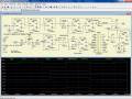
BTW, I updated the schematic to show the replacement of the 2-input AND gates with 3-input ANDs; also cleaned up the signal names a bit. See the attached. To show the bslow delay, I increased the clka to 3.2kHz and clkb to 100hz; and just zoomed in on a portion so the delay could be clearly seen.

You may be wondering what the item with the label of VUE1 does; it takes logic-level inputs and provides outputs that are offset from each other by ~1v, and about 500mV in amplitude. The signal out names have to be different than the signal in names. Without that tool, it would be very difficult to display more than a few logic waveforms on the output plots without making the display unintelligible.
 

Attachments

Top