What Ron H is proposing is essentially the same thing as biasing a BJT transistor so the signal is in the operating area.
This "moves" the entire signal from -ve to +ve to be entirely +ve, the signal then goes through the delay, and at the output, another capacitor removes the bias applied so the delay could function, leaving an AC -ve to +ve signal.
If you tried to amplify the -ve to +ve signal, the BJT transistor would only amplify the +0.6V to +ve portion, since any lower voltages would turn the transistor off entirely. This is the problem you are seeing with your current attempt of a BBD.
Think of a sinewave alternating from +1V to -1V, if you feed that through a capacitor, which is connected to a voltage divider, the -1V to +1V AC signal then becomes a 0 to 2V signal, this can be amplified, delayed, or any other action, then the output goes through another capacitor to remove the +1V "DC Bias" from the signal, resulting in a -1V to +1V Sinewave.
Since semiconductors are generally polarized (only work with positive voltages or only negative voltages) this issue comes up frequently.
There are more elaborate and accurate methods, such as an op amp to add the bias, but for simple signals, capacitor coupling suffices.
I have quoted your post, thatoneguy, as i realized that my NMOS transistors are opening their gates from the clock voltage. Which means, when the clock goes high, the transistor gate is fully open and hence the channel is conducting. Now, if my signal has both the +ve and -ve components, then it should be able to pass via the channel from source to drain along the BBD line? What do you say?
I am saying this, because, disregarding my signal i.e action potential, for time being, i tried only positive signal. Like pulses, but only in +ve peaks. The BBD delay still doesn't work. All i am seeing is the clock spikes at the output.
I have not yet implemented the sample and hold as suggest by Ron H.
So please, can you clarify that what circuit i should add at the output line, i.e the last source or drain contact on the last transistor?
I am NOT asking for a schematic, but just the circuit name so i can search it up. I did try the source follower as Ron H suggest, but it didn't work.
I have quoted your post, thatoneguy, as i realized that my NMOS transistors are opening their gates from the clock voltage. Which means, when the clock goes high, the transistor gate is fully open and hence the channel is conducting. Now, if my signal has both the +ve and -ve components, then it should be able to pass via the channel from source to drain along the BBD line? What do you say?
I am saying this, because, disregarding my signal i.e action potential, for time being, i tried only positive signal. Like pulses, but only in +ve peaks. The BBD delay still doesn't work. All i am seeing is the clock spikes at the output.
I have not yet implemented the sample and hold as suggest by Ron H.
So please, can you clarify that what circuit i should add at the output line, i.e the last source or drain contact on the last transistor?
I am NOT asking for a schematic, but just the circuit name so i can search it up. I did try the source follower as Ron H suggest, but it didn't work.
Have you tried taking your work so far to your professor (or one of his grad students), explain your problem, and get advice? That is their purpose in life.
Have you tried taking your work so far to your professor (or one of his grad students), explain your problem, and get advice? That is their purpose in life.
Actually i have, but my contact time with him is limited and i need to complete this project soon enough. For analog delay, BBD seems to be the only practical approach that could be implemented on a CMOS. I would do it digitally in no time, but like i have said, it would consume more power and would be more complex to implement on a custom IC design.
Now, BBD has been implemented before and worked, so my question is where could i be going wrong?
Actually i have, but my contact time with him is limited and i need to complete this project soon enough. For analog delay, BBD seems to be the only practical approach that could be implemented on a CMOS. I would do it digitally in no time, but like i have said, it would consume more power and would be more complex to implement on a custom IC design.
Now, BBD has been implemented before and worked, so my question is where could i be going wrong?
Also, like i mentioned in my post, i am not even trying my action potential signal. I am just trying to delay a signal that is only positive in amplitude.
Also, like i mentioned in my post, i am not even trying my action potential signal. I am just trying to delay a signal that is only positive in amplitude.
No. What would be the point in me clarifying it one more time? I obviously don't know how to explain it so that you can understand it.
You find all the relevant material that I posted, and tell us what parts you don't understand. Maybe I, or one of the other members, will be able to say it in a way that you understand, or clear up some particular point(s).
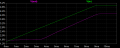
Here is something you can try. On your BBD simulation, apply a PWL ramp to the input that goes from 0V to 5V in 10 milliseconds.
Run the simulation for 12 milliseconds.
Plot the input and output waveforms on the same graph. This will show you the linear range of your BBD in simulation (hardware will probably be at least a little bit different).
When I did this on my BBD sim, the output was fairly linear over an input range of 3.2V to 5V. However, the output voltage over that same input range went from about 2.1V to about 4.1V. You should be able to see from this that you cannot expect the input DC level to appear at the output. You should also be able to see that the circuit does not work with the input voltage below 3.2V.
I don't know why this is. I am not a BBD expert.
Here is something you can try. On your BBD simulation, apply a PWL ramp to the input that goes from 0V to 5V in 10 milliseconds.
Run the simulation for 12 milliseconds.
Plot the input and output waveforms on the same graph. This will show you the linear range of your BBD in simulation (hardware will probably be at least a little bit different).
When I did this on my BBD sim, the output was fairly linear over an input range of 3.2V to 5V. However, the output voltage over that same input range went from about 2.1V to about 4.1V. You should be able to see from this that you cannot expect the input DC level to appear at the output. You should also be able to see that the circuit does not work with the input voltage below 3.2V.
I don't know why this is. I am not a BBD expert.
What a coincidence. I just did this simulation with my supervisor. The thing is, our signal is +ve 5v at the moment, just for testing purposes. The clocks are also 5v. So i don't have input voltage below 3.2.
Now if i understand what you said, basically you are saying, for the part of the signal which is less than 3.2volts +ve, i will need to make sure that DC offset is atleast 3.2? Right?
What a coincidence. I just did this simulation with my supervisor. The thing is, our signal is +ve 5v at the moment, just for testing purposes. The clocks are also 5v. So i don't have input voltage below 3.2.
Now if i understand what you said, basically you are saying, for the part of the signal which is less than 3.2volts +ve, i will need to make sure that DC offset is atleast 3.2? Right?
As I said, run the input ramp from 0V to 5V. Find the linear part of the output waveform. Offset your your input signal so that the p-p signal fits into that range. On my sim, the linear range started at 3.2V. On yours, it may be different. I'm sure you are not using the same transistor models as I am.
You should probably amplify your action potential so that it occupies most of the linear range. Since the BBD introduces a fixed amount of noise (mostly clock noise), your output signal-to-noise ratio will be optimized under this condition. The down side of this is that any nonlinearity in the output will cause more distortion on a high amplitude signal than on a low amplitude one.
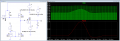
Also, the source follower/sample and hold will remove a lot of clock noise, reducing output filtering requirements. See the attachment. The top waveform is the output of the source follower. The bottom waveform is the output of the S&H. Be aware that you will need some sort of output buffer. The S&H output cannot drive an external load. I would probably try a PMOS source follower.
As I said, run the input ramp from 0V to 5V. Find the linear part of the output waveform. Offset your your input signal so that the p-p signal fits into that range. On my sim, the linear range started at 3.2V. On yours, it may be different. I'm sure you are not using the same transistor models as I am.
You should probably amplify your action potential so that it occupies most of the linear range. Since the BBD introduces a fixed amount of noise (mostly clock noise), your output signal-to-noise ratio will be optimized under this condition. The down side of this is that any nonlinearity in the output will cause more distortion on a high amplitude signal than on a low amplitude one.
Also, the source follower/sample and hold will remove a lot of clock noise, reducing output filtering requirements. See the attachment. The top waveform is the output of the source follower. The bottom waveform is the output of the S&H. Be aware that you will need some sort of output buffer. The S&H output cannot drive an external load. I would probably try a PMOS source follower.
He posted how his quickly simulated circuit responded in order to show you HOW to perform the simulation he is referring to. He isn't using Cadence, and doesn't have your transistor models. Those parts don't matter at this level. Ron H is teaching you the methods for finding out what you need.
Think of it as Ron showing you how to write a datasheet for your BBD when you are finished, except you need to substitute in YOUR transistor sizes/values and response, rather than his.
He posted how his quickly simulated circuit responded in order to show you HOW to perform the simulation he is referring to. He isn't using Cadence, and doesn't have your transistor models. Those parts don't matter at this level. Ron H is teaching you the methods for finding out what you need.
Think of it as Ron showing you how to write a datasheet for your BBD when you are finished, except you need to substitute in YOUR transistor sizes/values and response, rather than his.
I know i know. I am just clarifying. LT Spice is not as higher-level simulator as CadenceVirtuoso.
My project is not just getting the analog delay to work, but the fact that it should work in Cadence, which we will then transfer to a layout where i will have to actually design how each minute component of each individual component, like NMOS transistors, is connected to others. So that means i will have to define the metal, the poly-silicon, the doping down to the real time levels and then send it off to a Fab. Think of this project as me designing my own BBD chip, the only difference being that those old MN/TDA/SAD series BBD chips were built on Fab processes pretty old by what i have at my disposal. But then i have to implement my BBD line with other systems, like the amplifiers and such. So it really is a custom IC.
Cadence is a good software for such work. However, sometimes it will give you ridiculous results that shouldn't be there. Like every CAD suite, it has it's downsides. That is why i keep asking Ron H about his LT Spice simulation. So i can analyze and know if it's me doing something wrong, or is it Cadence playing tricks.
Trust me, i implemented the entire design that Ron H showed in his LTSpice schematic in Cadence, and it didn't work. That is why i kept asking about the input DC offsets and the output source followers and the sample and hold.
So while i am still struggling with this project, i was wondering if Ron H and thatoneguy, if you could please have a look at this pdf document, which is the original paper from F.L.J.Sangster who invented the BBD.
On page 3 he shows the circuit for the MOS BBD.
Now, if i am correct, in the schematic, he shows the AC signal (with the AC wave thing), then if i am correct, a DC Bias, but in this case negative as he is using PMOS. Then you have the normal BBD, and finally towards the left, at the output, he has shown the source follower tapped out to a load, i am assuming it's a resistor or some load impedance?
Then the drain voltage is -ve as well, as this is PMOS.
What do you say, i think i should try using PMOS instead of NMOS?
I think they used PMOS because the PMOS process was developed before NMOS.
I remember back in the mid '60's, I was working for a company called General Microelectronics.. We had a contract to develop a 41 stage linear feedback shift register. Our technology was PMOS. That's all we had. I suspect the first BBD devices were done in PMOS for the same reason.
There is no good reason I can think of to use PMOS. You are already trying to use a device that has been obsolete for about 30 or 40 years. Don't compound it by using inferior transistors. NMOS transistors have about 3 times the mobility of PMOS. I don't know if that helps, but I don't think it will hurt.
The delay is not much as i am using only 20 stages, but it is something. I discussed with my supervisor, and he says it might be a good idea to move on to the next stage, i.e designing a threshold circuit to detect the action potential at a certain voltage and trigger the Sigma-Delta ADC which i have to design next.
I am looking for a simple comparator circuit like in a op-amp, for threshold. You think that is the right direction?
Any suggestions would be welcome. Also, ADC has to be basic 10 bit Sigma Delta.

 Facebook
 Google
 GitHub
 Linkedin