 Facebook
 Google
 GitHub
 Linkedin
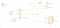
So I was looking back at the original schematic that I'd reverse engineered and got to wondering about the path for the clock signal.
While several ICs (CPU, 6840 timer IC, 6821 PIA, and the lower half of RAM) are driven directly from the 1MHz oscillator, other parts of the clock signal path are combined with other signals:
The chip select for the ROM is generated by a NAND of the A15 address line and the clock.
The chip select for the 6840 and 6821 ICs is generated by NAND of the clock and A15 (inverted).
The clock bus that continues to the interface board is fed through a NAND gate with the reset line.
On the interface board, this modified clock goes directly to the upper half of RAM.
The clock for the 8279 display / keyboard driver is fed through a 74LS375 latch.
The circuit that splits the R/W line into separate /RD and /WR lines for the 8279 is also OR'd with the clock.
Is there a reason for all this, or did someone overthink the design? (see attachment for a simplified schematic of my post)
Attachments
-
 252.1 KB Views: 23


