Class D amplifier Schematic.

Thread Starter

Hassan Wahaj Malik

Joined Oct 15, 2017
45
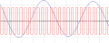
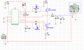
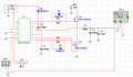
The simulation for the following circuit is not working. i am feeding in a PWM input to the class D amplifier and then converting it back to an analog signal by a low pass filter. I am unsure whether it is due to the connection of Vb and Vs?
 

Attachments

crutschow

Joined Mar 14, 2008
34,282
Not surprising it doesn't work.
The IR2010 data sheet clearly shows the bootstrap connection needed (Vb and Vs) to drive the top N-MOSFET (below).
(The N-MOSFET gate must be driven at least 10V above its drain voltage to fully turn on).
Why did you think the circuit would work without that? :confused:

upload_2017-10-21_19-45-20.png
 

Thread Starter

Hassan Wahaj Malik

Joined Oct 15, 2017
45
Isn't the gate voltage determined by the incoming signal? which for my case would be a PWM signal. I would not be using the comparator that is the reason i grounded it. I don't get what you're saying. Could you please explain it further?
 

crutschow

Joined Mar 14, 2008
34,282
Isn't the gate voltage determined by the incoming signal? which for my case would be a PWM signal.
No. the value of the gate voltage is different from the incoming signal voltage
The gate should be turned on and off (acting as a switch) by the incoming digital signal.

The PWM duty-cycle just determines how long it is on and how long it is off.
The analog value is the average value of the on and off period.

To turn off the N-MOSFET its Vgs should be near 0V.
To turn it fully on Vgs should be ≥+10V.
 

crutschow

Joined Mar 14, 2008
34,282
I have attached the pin layout. Could you please tell me how i should configure it? i am stuck on it since a week. I am having a hard time figuring out how i should design it. thanks.
Did you not look at the diagram in post #2?
Just look both diagrams to determine the pin-out versus function.
I'm too lazy to do that simple task for you. :rolleyes:
 

Ylli

Joined Nov 13, 2015
1,086
Looking at the data sheet for the IR2010, it appears to me that the HIN and LIN inputs go directly to schmitt triggers. These are not linear inputs. I don't see how you can use this chip to impose a linear signal onto a pulse stream.
 

crutschow

Joined Mar 14, 2008
34,282
Why is D1 a Zener?
It should be a small Schottky diode.

Why do you have a voltage source (V4) at Q2's source?
Normally that source terminal goes to ground.

I don't understand why you are modifying the circuit shown in the data sheet.
Since you don't seem to really understand how the circuit works, why would you make changes to it? :confused:
I am getting this at the output but the analog signal dies out at the end. I have attached the result and the schematic
That PWM in post #8 shows no modulation (variation in pulse duty-cycle), so would give only a DC output.
I don't see how you can use this chip to impose a linear signal onto a pulse stream.
It's a PWM signal modulated from an analog waveform.
That average value of a PWM signal equals the input modulated signal.
Look up PWM if you don't understand.
 

dendad

Joined Feb 20, 2016
4,451
Are you driving it with an audio encoded PMW signal?
This chip is not an analog to PWM converter.

And I reckon you need an inverter between Hin and Lin. As it is, you are trying to switch the top and bottom FETs on together if I remember the data sheet correctly.

Yes, I agree with cruschow, D1 should not be a zenner but a Schottky diode. And get rid of the 15V on Q2. just put it to gnd.
 
Last edited:

Ylli

Joined Nov 13, 2015
1,086
It's a PWM signal modulated from an analog waveform.
That average value of a PWM signal equals the input modulated signal.
Look up PWM if you don't understand.
Yes, I know what PWM is. You are not going to linearly modulate pulse width by feeding the analog modulating signal into a digital gate.

Best you are going to see here is an output pulse frequency equal to the analog input frequency with a pulse width output proportional to the DC offset of the analog signal. And you would need an inverter between the HIN and LIN inputs to even get that.
 

Thread Starter

Hassan Wahaj Malik

Joined Oct 15, 2017
45
Are you driving it with an audio encoded PMW signal?
This chip is not an analog to PWM converter.

And I reckon you need an inverter between Hin and Lin. As it is, you are trying to switch the top and bottom FETs on together if I remember the data sheet correctly.

Yes, I agree with cruschow, D1 should not be a zenner but a Schottky diode. And get rid of the 15V on Q2. just put it to gnd.

yes i have will drive it with an audio encoded PWM signal.
 
Top