Circuit Works on Breadboard But Not PCB

Thread Starter

ryan1

Joined Jun 16, 2020
23
Hello all!

I've been trying to send and receive a signal by using TOSLink optical transmitters and receivers from Sys-Concept in the same circuit (making a transceiver of sorts):

http://www.sys-concept.com/toslink_receiver.htm

According to the data sheets of both the receiver and the transmitter, I need a bypass capacitor between each power/ground pins of each part. I am sending my signals over the TTL interface of a Tinkerforge bricklet:

https://www.tinkerforge.com/en/doc/Hardware/Bricklets/RS232_V2.html

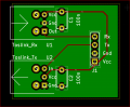
I managed to send and receive signals just fine when I make the circuit on a breadboard. However, when I made a PCB (photo attached), the receiver just gets a stream of gibberish. U$1 is the receiver, and U$2 is the transmitter. There's a 4-pin connector (on the right) that connects the board to the Tinkerforge TTL interface. Does anyone know what I'm doing wrong? I'm a little new to this stuff, and I've been stumped for a while. I hoping that it's just a careless error I've overlooked.

Capture.JPG
Thank you! I'm happy to provide any more information that is needed.

Sincerely,
Ryan
 

jpanhalt

Joined Jan 18, 2008
11,087
Maybe too obvious, but were your holes plated or did you solder to both sides of the board?
Do you have a ground plane for the capacitors?
Please label VCC, GND, and Signal.
 

Thread Starter

ryan1

Joined Jun 16, 2020
23
Thanks for the response. The through holes for the components look like they're plated, and I confirmed this with a multimeter, so I didn't solder to both sides of the board. I don't have a ground plane for the capacitors. Would that help? I didn't think I would need one.

1593117864287.png
 

Irving

Joined Jan 30, 2016
3,843
Slightly confusing - is this top or bottom view? silkscreen for caps implies top, but that for connector suggests bottom... or maybe connector is mounted on underside of board?

Anyway, assuming view is top of board, layout looks ok, so problem must be in PCB (missed/damage 'via' as said above) or physical connections.

Would have been good to put Vcc, Gnd, In, Out on silkscreen too (I know its there faintly on pads on layout but doesn't hurt to be explict), and RX TX by devices - all helps with troubleshooting.

I would have liked to have seen heavier tracks for VCC and a Ground Plane on the underside of PCB, there no reason not to.

Data sheets show isolating 47uH inductor in VCC line to receiver, and some very specific PCB layout info, how critical that is isn't obvious.

One last point... decoupling caps must be in the path from supply to device, not hung off the side, otherwise no point in them being there. So the Vcc route for Tx is OK, but Rx effectively has no decoupling (and in reverse for the Gnd line) In fact if you're transmitting and receiving simultaneously I wouldn't be surprised if that's ffffcausing cross-talk between Tx and Rx.

1593117544408.jpeg
 
Last edited:

Thread Starter

ryan1

Joined Jun 16, 2020
23
The picture I posted is a top view of the board--the capacitors and transmitter/receiver are mounted on the top, wheres the connector is mounted on the underside of the board. Sorry for the confusion!

I believe the 47 mH inductor is needed for the Mini Toslink Receiver, which I am not using. I'm using the 16 Mbps Toslink Receiver.

For ease of access, here are links to the PDF data sheets of the receiver and the transmitter I am using:
Receiver: http://www.sys-concept.com/toslink_receiver_files/Toslink-RX-Data-16Mbps-Sys.Concept.pdf
Transmitter: http://www.sys-concept.com/toslink_receiver_files/Toslink-TX-Data-16Mbps-Sys.Concept.pdf

I did notice that the receiver data sheet does suggest to attach a 30 pF capacitor between V_OUT (which is the RX pin) and ground to avoid "loading effect." Is this critical? I don't have the 30 pF capacitor on my breadboard, and the circuit works fine. There was another project online that used TOSLink transmitter/receivers for a CNC, and they didn't use a 30 pF capacitor.

I'm not sure if a ground plane is necessary, but it might help. Not sure if that'll resolve my problems, though, so any more suggestions would be awesome. Thank you!
 

nsaspook

Joined Aug 27, 2009
13,079
Device power decoupling caps must be in A low impedance signal path from device power pins to device common pins.

I've never heard this as a rule, while it might often be the case.

"One last point... decoupling caps must be in the path from supply to device, not hung off the side, otherwise no point in them being there."
 

Thread Starter

ryan1

Joined Jun 16, 2020
23
Hmmm ok. Maybe I'll try cutting some traces and adding some jumper wires. I tried replicating the problem on the breadboard, but it still works on the breadboard even when the decoupling caps aren't in the path from the supply to the device. The receiver shows a bunch of gibberish when I just plug in the PCB (before I even try to transmit any data), so the noise occurs even without trying to simultaneously transmit and receive.
 

Thread Starter

ryan1

Joined Jun 16, 2020
23
Unfortunately, cutting the traces and adding the jumper wires to make sure the decoupling caps are in the path from the supply to the device didn't work. Thanks for the advice, though! Any other thoughts?
 

Thread Starter

ryan1

Joined Jun 16, 2020
23
Things I thought might be worth mentioning:

1. I've tried doing a transmitter separately and a receiver separately on different perfboards, and both times they worked fine.
2. I don't have a 30 pF bypass capacitor to put between RX and GND (to avoid loading effect), but I used a 330 pF capacitor instead. Still receiving the same stream of gibberish. Will probably get some 30 pF bypass capacitors next Monday, but I don't think they are the issue...

Had a question, too, if anyone could answer. If, say, I use a ground plane for my capacitors and the PCB worked, why would the breadboard be working if it doesn't have a ground plane? Thought I would ask because I wanted to save having to make another PCB as last resort due to the ~1 week turnaround time.
 

sparky 1

Joined Nov 3, 2018
756
We have all had this happen,
I have epoxied a smaller board, it takes some thought but if done neatly it looks ok. really frustrating to mess with nice board.
The ferrite beads also mop up parasitics,again epoxy small pad start dropping them on a wire. parasitics and ground planes.
small capacitors, pulling ceramic and going with tantalum. Decrease noise. What is going on right outside the integrated circuit should not overshadow what is going on inside the IC or component it effects the signal. You are providing a path away from instead of letting it hang out on the pins or other parts. I use an amplified probe to locate then what effect a ground probe tells me where more decoupling is necessary. There is some sense of satisfaction eliminating gremlins.
 
Last edited:

Daniel462

Joined Nov 29, 2019
1
The datasheet you included of the receiver writes that it needs a supply voltage of +5VDC. The transmitter on the other hand can have a supply voltage between +3VDC and +5VDC. The Tinkerforge unit uses 3V3 TTL.
1593162569186.png

According to your PCB silkscreen you are using a 3.3VDC supply voltage.

I don't know how your setup is on the breadboard, but this is something that I noticed. Hope it helps :)
 

Irving

Joined Jan 30, 2016
3,843
Yes, many times what worked as a lashup didn't on a PCB. I've learnt the hard way over many years that decoupling can be more an art form than science, but on the whole its better to put it in and not need it than not and find you do. But its only worth it if the cap is as close to the chip Vcc pin as possible, especially where high speed and fast rise/fall times are present, together with low impedance ground planes, MLCC capacitors (pref SMD) and shorter fatter supply tracks where possible to minimise stray inductances. Now, I'm not saying your PCB needs that, but adopting good practice never hurts. These days PCB costs from the likes of jlcpcb (other pcb manufacturers are available) are minimal, no more costed by the amount of copper, so more and more I'm using 4-layer boards to minimise routing as my time costs far more to spend an extra couple of hours trying to find a route for that last Vcc track!

Anyway, here's my version of your board. Note the ground plane so now theres only 4 traces to route. I've opted to keep the Vcc supply to Tx as short as possible as thats the one likely to be generating most noise. I'd probably move the connector even closer to the active parts. Note the smaller ceramic caps, much better for decoupling as have very low ESR, and right up against device, keeping Vcc to device as short as possible. Now the cap is doing its job, providing local stored energy to the device, holding up Vcc despite any effects of the inductance of the longer Vcc input track. Just because your device is rated at 10ma Vcc that's rms, the peaks could be much higher.

1593174261673.png

Edit: Just seen the pevious post ref 3.3v v 5v - that could certainly be an issue, but plenty of space on board for level translation & local regulator or 1 chip boost converter. Many options...
 

Attachments

Last edited:
If there is any consolation, I can assure you that most, if not all, of the more knowledgeable experts in this forum have had a board which doesn't work due to layout issues.

Fortunately yours is a small, simple board. But I've had to redo very complex boards in which 95% of everything is working correctly but a function tucked in a board's corner refuses to do so.
It is heartbreaking and many times very hard on your wallet, but painful experience is the best way to learn.
 

Thread Starter

ryan1

Joined Jun 16, 2020
23
I'm truly baffled now. While I was waiting for the new PCB, I replicated the circuit on a perfboard, attached a 30 pF bypass capacitor between ground and RX, powered the whole board on 3.3 V, and everything worked! However, I recently got the new PCBs, wired up the same circuit (except with smaller ceramic capacitors), added the same 30 pF bypass capacitor, and attached the PCB directly to my Tinkerforge RS232 bricklet via the rectangular connector. It doesn't work. Nevertheless, very strangely, when I connect the bricklet to my PCB connector via some longer breadboard cables, everything works! The perfboard I made similarly had relatively long wires (<5 cm) to connect the circuit to the bricklet. It seems that when the PCB is farther away from the bricklet, it appears to work.

This has sort of stumped me. Does anyone know why this happens, and if there is a workaround so I can directly connect the PCB to the Tinkerforge bricklet? I tried covering the leads with tape, but with no success.
 

Thread Starter

ryan1

Joined Jun 16, 2020
23
This is the configuration that doesn't work for some reason, where the PCB is directly plugged into the bricklet. I tested the resistance between the header connector on the bricklet and the corresponding socket connector on my PCB, and there was nothing out of the ordinary (less than one Ohm resistance).
 

Attachments

Thread Starter

ryan1

Joined Jun 16, 2020
23
Are you sure you're not shorting something, perhaps with the standoffs.

Just thinking out loud here...because I have done exactly that.
I don't think it's that because I tried running it without the standoffs, and it doesn't work. Thanks for the thought though!
 

Irving

Joined Jan 30, 2016
3,843
Very strange indeed!

Does your earlier PCB show the same phenomenon when on longer cables?

Are you 100% sure there is no contact between board components when the 2 are mated?

Do the standoffs link the boards electrically? What happens if you mate them without the standoffs? Ah, you tried that already...

Can you try with a very short cable. If you remove connectors and hardware with direct wires does it behave?

What is under the TOS receiver on the other board?
 
Last edited:
Top