Circuit debugging help needed

Thread Starter

mishra87

Joined Jan 17, 2016
1,034
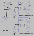
Could anybody help me to understand the attached circuit.
Note this circuit is working in production but i do not understand.

Both two set up of circuit is just replica of each other.

what is role of R3 and R8 and why it is connected with source of M1 and M2.

If i removed M2 and its driving associated circuit and connect M1 source to GND the first circuit is not working.

Could anybody explain the working of this circuit.
 

Attachments

Thread Starter

mishra87

Joined Jan 17, 2016
1,034
It would help if we knew what the purpose of the circuit is.
How is it "working"?
Is R5 the output load resistor?
Thank you so much all for your suggestion.
In place of R5 a DC motor is used and hole circuit is used to drive the DC motor.
I am not much aware of DC motor working if it working bi-direction or unidirectional.

I tired to run motor using only one set of driver circuit but it did not work then i draw the 2nd part which is already in schematic and now the with complete circuit it works.

Yes, It worked but now i do not understand the working of this circuit and the purpose of this complicated circuit.

coz M1 and M2 gate and source are at same potential.

Regards,
 

Thread Starter

mishra87

Joined Jan 17, 2016
1,034
R3 and R4 should not be in parallel. There may be other issues but I stopped when I spotted that.
The circuit is correct and working well in production.
Theoretical i do not understand the behavior and reason to use this complicated circuit
 

MrAl

Joined Jun 17, 2014
11,342
The circuit is correct and working well in production.
Theoretical i do not understand the behavior and reason to use this complicated circuit

Looks to be just a MOSFET half bridge driver circuit with the MOSFETs but is not exactly drawn right.
The lower pulse should at least be the invert of the upper pulse with some added dead time but it is not drawn that way it is drawn as a parallel mosfet driver but with mosfet half bridge output which does not work it will blow both mosfets.

So if the upper pulse goes from t=0 to t=20us for example, then the lower pulse should go from 20us to 40us for example in theory for a 50 percent duty cycle. But in practice the upper pulse would go more like from 0 to maybe 16us and the lower pulse from 20us to 36us which would mean a 4us dead time. The dead time is related to the actual turn off time of the two MOSFETs, for longer turn off times you need longer dead time or else you will see a destructive power supply punch through.
 

AnalogKid

Joined Aug 1, 2013
10,971
R3 and R8 each drop voltage when Q1/Q2 passes current, so that the FET gate voltage is above the source voltage to turn the FET on.
Nope. R3 and R8 assure that each FET turns *off* completely and quickly when V1 and V5 are high. This reduces the power dissipation (and operating temperature) of the FETs. They do not affect the values of the gate voltages when V1 and V5 are low and Q1 and Q2 are on.

ak
 
Last edited:
Top