Can we use this 4 bit adder commercially?

WBahn

Joined Mar 31, 2012
32,703
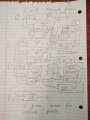
I wonder if I can get any money for this circuit design.
Why do you think that you can get money for it? What is new and useful about it? What is the comparison between it and other four-bit adders that reveals that it brings something worthwhile to the table?

You claim that it has four gate delays for it's critical path. What is that critical path? If I understand your (very sloppy) logic diagram, your critical path is XOR->AND->OR->XOR. But how many gate delays is each of those gates? Depending on how they are implemented, they each have at least two gate delays (a gate delay is generally the propagation delay for a two-input NAND gate in a given technology, though there is no exact and universally-agreed upon definition).
 

WBahn

Joined Mar 31, 2012
32,703
Mmmmmmh well I do own the intellctual property rights.
You own the intellectual property rights to a lookahead adder?

Just how old are you?

These adders date back to Zuse in the 1930s (first implementation) and, conceptually, to Babbage in the mid-1800s.

IBM took out a patent in nearly seventy years ago.

So just what intellectual property rights associated with them are you claiming to own?
 

Thread Starter

micoffey

Joined Aug 10, 2025
17
Ugh, you can take it up with the UC at Santa Barbara that came up with it. They said it worked and gave me credit for it.
 

Thread Starter

micoffey

Joined Aug 10, 2025
17
Why do you think that you can get money for it? What is new and useful about it? What is the comparison between it and other four-bit adders that reveals that it brings something worthwhile to the table?

You claim that it has four gate delays for it's critical path. What is that critical path? If I understand your (very sloppy) logic diagram, your critical path is XOR->AND->OR->XOR. But how many gate delays is each of those gates? Depending on how they are implemented, they each have at least two gate delays (a gate delay is generally the propagation delay for a two-input NAND gate in a given technology, though there is no exact and universally-agreed upon definition).
What kind of engineer are you? Gate delays for gate delays? You obviously have a different definition of gate than us.
 

Thread Starter

micoffey

Joined Aug 10, 2025
17
Why do you think that you can get money for it? What is new and useful about it? What is the comparison between it and other four-bit adders that reveals that it brings something worthwhile to the table?

You claim that it has four gate delays for it's critical path. What is that critical path? If I understand your (very sloppy) logic diagram, your critical path is XOR->AND->OR->XOR. But how many gate delays is each of those gates? Depending on how they are implemented, they each have at least two gate delays (a gate delay is generally the propagation delay for a two-input NAND gate in a given technology, though there is no exact and universally-agreed upon definition).
Just take a look at the adder. It uses or and and gates. It only has basic gate delays. Its critical path is 4 gates, better than the leading competitor we found on StackExchange.
 

spenkmo

Joined Apr 24, 2025
25
Here is a two level implementation. For simplicity, I just show S3 below. If the inverted input must be counted as a level, then this is a three level implementation.
S3 = ~A0&~A1&~A2&~A3&~B0&~B1&~B2&B3 | ~A0&~A1&~A2&~A3&B0&~B1&~B2&B3 | ~A0&~A1&~A2&~A3&~B0&B1&~B2&B3 | ~A0&~A1&~A2&~A3&B0&B1&~B2&B3 | ~A0&~A1&~A2&~A3&~B0&~B1&B2&B3 | ~A0&~A1&~A2&~A3&B0&~B1&B2&B3 | ~A0&~A1&~A2&~A3&~B0&B1&B2&B3 | ~A0&~A1&~A2&~A3&B0&B1&B2&B3 | A0&~A1&~A2&~A3&B0&B1&B2&~B3 | A0&~A1&~A2&~A3&~B0&~B1&~B2&B3 | A0&~A1&~A2&~A3&B0&~B1&~B2&B3 | A0&~A1&~A2&~A3&~B0&B1&~B2&B3 | A0&~A1&~A2&~A3&B0&B1&~B2&B3 | A0&~A1&~A2&~A3&~B0&~B1&B2&B3 | A0&~A1&~A2&~A3&B0&~B1&B2&B3 | A0&~A1&~A2&~A3&~B0&B1&B2&B3 | ~A0&A1&~A2&~A3&~B0&B1&B2&~B3 | ~A0&A1&~A2&~A3&B0&B1&B2&~B3 | ~A0&A1&~A2&~A3&~B0&~B1&~B2&B3 | ~A0&A1&~A2&~A3&B0&~B1&~B2&B3 | ~A0&A1&~A2&~A3&~B0&B1&~B2&B3 | ~A0&A1&~A2&~A3&B0&B1&~B2&B3 | ~A0&A1&~A2&~A3&~B0&~B1&B2&B3 | ~A0&A1&~A2&~A3&B0&~B1&B2&B3 | A0&A1&~A2&~A3&B0&~B1&B2&~B3 | A0&A1&~A2&~A3&~B0&B1&B2&~B3 | A0&A1&~A2&~A3&B0&B1&B2&~B3 | A0&A1&~A2&~A3&~B0&~B1&~B2&B3 | A0&A1&~A2&~A3&B0&~B1&~B2&B3 | A0&A1&~A2&~A3&~B0&B1&~B2&B3 | A0&A1&~A2&~A3&B0&B1&~B2&B3 | A0&A1&~A2&~A3&~B0&~B1&B2&B3 | ~A0&~A1&A2&~A3&~B0&~B1&B2&~B3 | ~A0&~A1&A2&~A3&B0&~B1&B2&~B3 | ~A0&~A1&A2&~A3&~B0&B1&B2&~B3 | ~A0&~A1&A2&~A3&B0&B1&B2&~B3 | ~A0&~A1&A2&~A3&~B0&~B1&~B2&B3 | ~A0&~A1&A2&~A3&B0&~B1&~B2&B3 | ~A0&~A1&A2&~A3&~B0&B1&~B2&B3 | ~A0&~A1&A2&~A3&B0&B1&~B2&B3 | A0&~A1&A2&~A3&B0&B1&~B2&~B3 | A0&~A1&A2&~A3&~B0&~B1&B2&~B3 | A0&~A1&A2&~A3&B0&~B1&B2&~B3 | A0&~A1&A2&~A3&~B0&B1&B2&~B3 | A0&~A1&A2&~A3&B0&B1&B2&~B3 | A0&~A1&A2&~A3&~B0&~B1&~B2&B3 | A0&~A1&A2&~A3&B0&~B1&~B2&B3 | A0&~A1&A2&~A3&~B0&B1&~B2&B3 | ~A0&A1&A2&~A3&~B0&B1&~B2&~B3 | ~A0&A1&A2&~A3&B0&B1&~B2&~B3 | ~A0&A1&A2&~A3&~B0&~B1&B2&~B3 | ~A0&A1&A2&~A3&B0&~B1&B2&~B3 | ~A0&A1&A2&~A3&~B0&B1&B2&~B3 | ~A0&A1&A2&~A3&B0&B1&B2&~B3 | ~A0&A1&A2&~A3&~B0&~B1&~B2&B3 | ~A0&A1&A2&~A3&B0&~B1&~B2&B3 | A0&A1&A2&~A3&B0&~B1&~B2&~B3 | A0&A1&A2&~A3&~B0&B1&~B2&~B3 | A0&A1&A2&~A3&B0&B1&~B2&~B3 | A0&A1&A2&~A3&~B0&~B1&B2&~B3 | A0&A1&A2&~A3&B0&~B1&B2&~B3 | A0&A1&A2&~A3&~B0&B1&B2&~B3 | A0&A1&A2&~A3&B0&B1&B2&~B3 | A0&A1&A2&~A3&~B0&~B1&~B2&B3 | ~A0&~A1&~A2&A3&~B0&~B1&~B2&~B3 | ~A0&~A1&~A2&A3&B0&~B1&~B2&~B3 | ~A0&~A1&~A2&A3&~B0&B1&~B2&~B3 | ~A0&~A1&~A2&A3&B0&B1&~B2&~B3 | ~A0&~A1&~A2&A3&~B0&~B1&B2&~B3 | ~A0&~A1&~A2&A3&B0&~B1&B2&~B3 | ~A0&~A1&~A2&A3&~B0&B1&B2&~B3 | ~A0&~A1&~A2&A3&B0&B1&B2&~B3 | A0&~A1&~A2&A3&~B0&~B1&~B2&~B3 | A0&~A1&~A2&A3&B0&~B1&~B2&~B3 | A0&~A1&~A2&A3&~B0&B1&~B2&~B3 | A0&~A1&~A2&A3&B0&B1&~B2&~B3 | A0&~A1&~A2&A3&~B0&~B1&B2&~B3 | A0&~A1&~A2&A3&B0&~B1&B2&~B3 | A0&~A1&~A2&A3&~B0&B1&B2&~B3 | A0&~A1&~A2&A3&B0&B1&B2&B3 | ~A0&A1&~A2&A3&~B0&~B1&~B2&~B3 | ~A0&A1&~A2&A3&B0&~B1&~B2&~B3 | ~A0&A1&~A2&A3&~B0&B1&~B2&~B3 | ~A0&A1&~A2&A3&B0&B1&~B2&~B3 | ~A0&A1&~A2&A3&~B0&~B1&B2&~B3 | ~A0&A1&~A2&A3&B0&~B1&B2&~B3 | ~A0&A1&~A2&A3&~B0&B1&B2&B3 | ~A0&A1&~A2&A3&B0&B1&B2&B3 | A0&A1&~A2&A3&~B0&~B1&~B2&~B3 | A0&A1&~A2&A3&B0&~B1&~B2&~B3 | A0&A1&~A2&A3&~B0&B1&~B2&~B3 | A0&A1&~A2&A3&B0&B1&~B2&~B3 | A0&A1&~A2&A3&~B0&~B1&B2&~B3 | A0&A1&~A2&A3&B0&~B1&B2&B3 | A0&A1&~A2&A3&~B0&B1&B2&B3 | A0&A1&~A2&A3&B0&B1&B2&B3 | ~A0&~A1&A2&A3&~B0&~B1&~B2&~B3 | ~A0&~A1&A2&A3&B0&~B1&~B2&~B3 | ~A0&~A1&A2&A3&~B0&B1&~B2&~B3 | ~A0&~A1&A2&A3&B0&B1&~B2&~B3 | ~A0&~A1&A2&A3&~B0&~B1&B2&B3 | ~A0&~A1&A2&A3&B0&~B1&B2&B3 | ~A0&~A1&A2&A3&~B0&B1&B2&B3 | ~A0&~A1&A2&A3&B0&B1&B2&B3 | A0&~A1&A2&A3&~B0&~B1&~B2&~B3 | A0&~A1&A2&A3&B0&~B1&~B2&~B3 | A0&~A1&A2&A3&~B0&B1&~B2&~B3 | A0&~A1&A2&A3&B0&B1&~B2&B3 | A0&~A1&A2&A3&~B0&~B1&B2&B3 | A0&~A1&A2&A3&B0&~B1&B2&B3 | A0&~A1&A2&A3&~B0&B1&B2&B3 | A0&~A1&A2&A3&B0&B1&B2&B3 | ~A0&A1&A2&A3&~B0&~B1&~B2&~B3 | ~A0&A1&A2&A3&B0&~B1&~B2&~B3 | ~A0&A1&A2&A3&~B0&B1&~B2&B3 | ~A0&A1&A2&A3&B0&B1&~B2&B3 | ~A0&A1&A2&A3&~B0&~B1&B2&B3 | ~A0&A1&A2&A3&B0&~B1&B2&B3 | ~A0&A1&A2&A3&~B0&B1&B2&B3 | ~A0&A1&A2&A3&B0&B1&B2&B3 | A0&A1&A2&A3&~B0&~B1&~B2&~B3 | A0&A1&A2&A3&B0&~B1&~B2&B3 | A0&A1&A2&A3&~B0&B1&~B2&B3 | A0&A1&A2&A3&B0&B1&~B2&B3 | A0&A1&A2&A3&~B0&~B1&B2&B3 | A0&A1&A2&A3&B0&~B1&B2&B3 | A0&A1&A2&A3&~B0&B1&B2&B3 | A0&A1&A2&A3&B0&B1&B2&B3
 

WBahn

Joined Mar 31, 2012
32,703
Just take a look at the adder. It uses or and and gates. It only has basic gate delays. Its critical path is 4 gates, better than the leading competitor we found on StackExchange.
I see several XOR gates in there. If you really only have OR and AND gates, then your circuit is not a valid binary adder since you are showing that the lsb of the output is then the OR of the lsbs of the two inputs, which is not correct.

You also seem to think that all gates have equal delay, which they don't. Why do we even bother with "gate delays"? Because it is a simple proxy for signal propagation delay. The only reason we care about propagation delay is because we want our circuits to be fast, which means that we need our gate delay proxy to reasonably relate to the actual propagation delay.

But in most (not all) logic families, and in particular in CMOS logic, which dominates current logic implementations, the AND and OR gates have about twice the propagation delay of the NOT, NAND, and NOR gates, hence they count as two gate delays each.

The XOR gate is a lot more variable because there are several ways to implement it. The direct implementation of the logic function has a propagation delay that is five times that of a NAND gate, Implemented using four NAND gates, it has three gate delays. Implemented directly in transistor-level CMOS, it still has two gate delays.

Your circuit is also not very useful because it is 4-bit only. It doesn't support carry-in or carry-out so that it can be used to create wider adders. There aren't that many applications these days that only need a four-bit adder and few of those really benefit from the speedup of a carry-lookahead approach compared to ripple-carry approach. The ripple-carry penalty becomes pronounced as the adder gets wider.

If you only want to look at propagation delay, then it is pretty trivial to design a 4-bit adder that has approximately the same delay as a single AND or OR gate. But speed isn't everything. You also need to look at size (number of transistors is the crude proxy for that) and power, particularly in today's battery-centric economy.
 

WBahn

Joined Mar 31, 2012
32,703

panic mode

Joined Oct 10, 2011
4,864
anything can be commercialized if someone will buy it. the only companies that would use something like this are IC manufacturers. logic ICs families and CPU/MCU are the only products that could use this.

but suppose this is a novel circuit and now that is shared online anyone can see it an try to use it. the question is how do you enforce intellectual rights? how do you find if anyone is using this design in their products? do you plan on buying any new MCU or CPU that enters the market, decap it, use electron microscope to inspect the die? or do you plan to use some backdoor to gain access to microcode? what if the user is some company in China? huge part of IC manufacturing is there and enforcing rights may be difficult. just saying...
 

Thread Starter

micoffey

Joined Aug 10, 2025
17
I see several XOR gates in there. If you really only have OR and AND gates, then your circuit is not a valid binary adder since you are showing that the lsb of the output is then the OR of the lsbs of the two inputs, which is not correct.

You also seem to think that all gates have equal delay, which they don't. Why do we even bother with "gate delays"? Because it is a simple proxy for signal propagation delay. The only reason we care about propagation delay is because we want our circuits to be fast, which means that we need our gate delay proxy to reasonably relate to the actual propagation delay.

But in most (not all) logic families, and in particular in CMOS logic, which dominates current logic implementations, the AND and OR gates have about twice the propagation delay of the NOT, NAND, and NOR gates, hence they count as two gate delays each.

The XOR gate is a lot more variable because there are several ways to implement it. The direct implementation of the logic function has a propagation delay that is five times that of a NAND gate, Implemented using four NAND gates, it has three gate delays. Implemented directly in transistor-level CMOS, it still has two gate delays.

Your circuit is also not very useful because it is 4-bit only. It doesn't support carry-in or carry-out so that it can be used to create wider adders. There aren't that many applications these days that only need a four-bit adder and few of those really benefit from the speedup of a carry-lookahead approach compared to ripple-carry approach. The ripple-carry penalty becomes pronounced as the adder gets wider.

If you only want to look at propagation delay, then it is pretty trivial to design a 4-bit adder that has approximately the same delay as a single AND or OR gate. But speed isn't everything. You also need to look at size (number of transistors is the crude proxy for that) and power, particularly in today's battery-centric economy.
Yeah, we <Mod: deleted obscenity >. There are xor gates in there.
 
Last edited by a moderator:

Thread Starter

micoffey

Joined Aug 10, 2025
17
anything can be commercialized if someone will buy it. the only companies that would use something like this are IC manufacturers. logic ICs families and CPU/MCU are the only products that could use this.

but suppose this is a novel circuit and now that is shared online anyone can see it an try to use it. the question is how do you enforce intellectual rights? how do you find if anyone is using this design in their products? do you plan on buying any new MCU or CPU that enters the market, decap it, use electron microscope to inspect the die? or do you plan to use some backdoor to gain access to microcode? what if the user is some company in China? huge part of IC manufacturing is there and enforcing rights may be difficult. just saying...
Usually, those IP rights are self enforced. IP theft can always be prosecuted. Besides, I don't have the money to patent it with the office right now.
 

Thread Starter

micoffey

Joined Aug 10, 2025
17
I see several XOR gates in there. If you really only have OR and AND gates, then your circuit is not a valid binary adder since you are showing that the lsb of the output is then the OR of the lsbs of the two inputs, which is not correct.

You also seem to think that all gates have equal delay, which they don't. Why do we even bother with "gate delays"? Because it is a simple proxy for signal propagation delay. The only reason we care about propagation delay is because we want our circuits to be fast, which means that we need our gate delay proxy to reasonably relate to the actual propagation delay.

But in most (not all) logic families, and in particular in CMOS logic, which dominates current logic implementations, the AND and OR gates have about twice the propagation delay of the NOT, NAND, and NOR gates, hence they count as two gate delays each.

The XOR gate is a lot more variable because there are several ways to implement it. The direct implementation of the logic function has a propagation delay that is five times that of a NAND gate, Implemented using four NAND gates, it has three gate delays. Implemented directly in transistor-level CMOS, it still has two gate delays.

Your circuit is also not very useful because it is 4-bit only. It doesn't support carry-in or carry-out so that it can be used to create wider adders. There aren't that many applications these days that only need a four-bit adder and few of those really benefit from the speedup of a carry-lookahead approach compared to ripple-carry approach. The ripple-carry penalty becomes pronounced as the adder gets wider.

If you only want to look at propagation delay, then it is pretty trivial to design a 4-bit adder that has approximately the same delay as a single AND or OR gate. But speed isn't everything. You also need to look at size (number of transistors is the crude proxy for that) and power, particularly in today's battery-centric economy.
It is a 4 bit only adder, but you can run wires from the carry variables to get their values.
 
Top