Can somebody explain about IR2101 working principle?

Thread Starter

EoGwangSeon

Joined Nov 14, 2019
3
2101_s.gif
<picture 1>
Hello I'm from South Korea. I need help about this circuit.
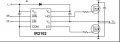
Picture 1 is typical connection about IR2101
ffzz.JPG
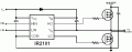
this is my circuit that i designed.
I want to know how it works. I want to know about working principle.
1. HIN = High, LIN = High -> Output "U" = ?
1. HIN = High, LIN = Low -> Output "U" = ?
1. HIN = Low, LIN = High -> Output "U" = ?
1. HIN = Low, LIN = Low -> Output "U" = ?


sorry about my english skill.
thank you for reading.
 

Attachments

Marley

Joined Apr 4, 2016
502
In your circuit you designed:
HIN is the logic level input to control the top MOSFET (M1). When high, the top MOSFET is switched on.
LIN is the logic level input to control the bottom MOSFET (M2). When high, the bottom MOSFET is switched on.
There is NO internal logic to prevent both MOSFETs switching on at the same time. SO BE VERY CAREFUL when using in an H-Bridge configuration.
The top MOSFET (M1) drain voltage can be up to 600V as the control signal is isolated internally. OK at 12V as in your design.
The top MOSFET (M1) needs a gate voltage higher than the supply to switch it on.
This voltage is created by the bootstrap diode (D6) and the bootstrap capacitor (C6).

Normal operation sequence:
  • Both inputs low - Both MOSFETS off. Voltage U not defined.
  • Input LIN high, HIN low - bottom MOSFET on. Voltage U is close to 0V. Capacitor C6 charges through D6.
  • This state needs to be long enough for C6 to fully charge.
  • Both inputs low for a short time to allow the bottom MOSFET to switch off. This is known as the "dead time".
  • Input LIN low, HIN high - top MOSFET switches on. Voltage U becomes close to the supply voltage (the voltage on the drain). The negative end of C6 also becomes this voltage. The positive end of C6 goes to the supply voltage plus 12V (24V in your circuit). Maintaining the positive gate voltage on the top MOSFET.
  • While this state is maintained, C6 slowly discharges. It is important that input HIN returns low before this capacitor discharges too much.
  • Both inputs now low for a short time to allow the top MOSFET to switch off. Another "dead time".
  • input LIN high, HIN low - bottom MOSFET on. Voltage U is close to 0V. Capacitor C6 charges through D6. The cycle repeats.

Important to realise that the top MOSFET cannot be on for a long time. C6 will discharge.
Also, in every cycle, the bottom MOSFET must be switched on to recharge C6 before the top MOSFET is used again.
Both MOSFETS must never be switched on at the same time!
 

Alec_t

Joined Sep 17, 2013
14,313
Both MOSFETS must never be switched on at the same time!
..... which means that HIN and LIN must never both be high at the same time. In practice you need to allow some 'dead time' between one of those inputs going low and the other one going high, because the FET gate capacitance takes a while to charge and discharge.
 

crutschow

Joined Mar 14, 2008
34,412
Operation of the charge pump:
  • When M1 is OFF and M2 is ON, the output U is low and capacitor C6 charges to near 12V through D6.
  • When M2 turns OFF and then M1 is turned ON, the voltage on C6 is applied through Vb between the gate and source of M!.
  • Since the bottom of C6 is connected to M1's source, the gate voltage will rise as the source voltage rises, keeping Vgs at 12V and M1 turned on as its source rises to the equal the drain voltage, and it is fully ON.
  • Diode D6 prevents C6 from discharging during this time.
 
Last edited:
Top