Buck regulator not able to reach full voltage

Status
Not open for further replies.

Thread Starter

liquidair

Joined Oct 1, 2009
208
I see issue with feedback trace being so close and parallel to the inductor.
Ya, the DS warns against this but I'm not sure what you are supposed to do there other than use a shielded inductor like I did and cover the trace with a ground plane. TI does the same thing on their EVAL boards however, and their Webench circuit has the FB trace directly under the inductor. I can see the only real thing to do is to rotate the inductor 90 deg counter-clockwise, but that forces the ground to be longer between the diode and Cout.

What would we see if that was an issue?

This looks like the same circuit on a TI forum
Yup it is. Figured I'd ask somewhere else since it seems the thread is dead.
 

Thread Starter

liquidair

Joined Oct 1, 2009
208
sounds like homework, is it?
No, not homework or school related. But it is my first foray into switching regulators so its all new to me. I tend to learn by studying a ton before I design the circuit, design and build thinking I understand and will have it work, have it not work and usually in some fantastic way, frantically search for answers for about 2 weeks, then find out it was a really dumb mistake I made. But by that time I have a pretty solid understanding of the concepts involved, lol.

Your switcher operates at about 260kHz. But what is your input frequency, 60Hz? Your schematic shows 15.5VAC input, but you don't list frequency unless this is a stepdown from MAINs so it'd be 60Hz. How smooth is the DC signal you have going into the switcher after all the filtering on the front end?
Ya, 60Hz mains so 120Hz. The DC is really smooth (can't see any ripple at 100mV), and I do see switching spikes on the input, but they are about 50mVpp. They appear to have some ringing on them actually.

I would recommend you first attempt using a car-battery at 12V for your input, so you have a solid DC input that can supply any level of current you desire, and see what happens to your output. Go from knowns. Don't change a lot of things, make an educated decision to change one thing, and then make a correct observation. Restore circuit state and try another educated decision, if the first didn't give you enough information.
This is good advice. I think the issue is this:
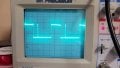
8VOutDiodeNodeLowVoltage.jpg

This is at the diode node. If I catch it really early I will see 2 spikes instead of one, indicating the switch only turns on every 3rd cycle. My guess is that if you averaged the voltage out over time you'd see it would add up to the output voltage I read at the same time on the DMM. So if the regulator tried to deliver 12V with this waveform, it would require double the current, and we'd run up against the current limit of the device, so of course we would see the voltage slowly rise and settle at some lesser value.

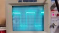
I can also get the full 12V instantly with the 220pF cap. A positive pulse appears where the spike is:
12VOutDiodeNode.jpg

This is clearly what we should see when the circuit is healthy. But the problem is that I can't rectify these two things in my head with my knowledge thus far. What does the switch not being able to turn on every other cycle and snubbing (I assume that is what the 220pF cap's function is when it works) have anything to do with each other? The only thing I can think of is some energy is released by the diode turning off that messes with switch controller in the IC and the 220pF then keeps that energy from getting to the IC...although I'm not sure why the diode's inherent 800pF wouldn't do that anyhow.

I could see ground bounce also messing with IC's switch controller doing this too, so I'm going to try to lower the ground impedance from input to output as crutschow suggested, but I also can't see why the 220pF cap would stabilize ground enough to restore order.
 

crutschow

Joined Mar 14, 2008
38,578
If a cap across the diode helps, then add a small resistor (start with about 50-100Ω) in series with the cap.
That gives you a typical snubber circuit with the resistor absorbing the energy of the spike/ringing.
 

Thread Starter

liquidair

Joined Oct 1, 2009
208
I just wanted to update this thread. Last week I got a thick piece of solid copper and used it to make a connection between the input and diode grounds like crutschow said and was able to witness a jump in the max voltage by about 1-2 volts but it wasn't enough.

I read some app notes that warned against filling the switch/diode/inductor node too much as this can radiate EMI and couple noise to the output, so I cut this down from a fill like I had to a fat trace. This actually made the max voltage considerably lower than before.

However, I used that piece of copper again and was able to get the full output immediately just by holding it in place. I attempted to solder it in place with no luck, and finally used some copper braid (solder wick) and it works now. The problem is that it is really finicky...the solder joints have to be just right, but it is working without the cap snubber now. So kudos to you crutschow and BobaMosfet!

For discussion, the issue appears to be the ground impedance was too high from the input and the diode ground...I tried to get too cute in controlling the current by making the connection through the IC pin. But given that it appears the impedance needs to be just right (as evidence by the solder joints being picky above), when I redesign this board, how can I be sure I've got the ground impedance low enough? Is there any optimum way to position the input cap?

Thank you again for your help crutschow and BobaMosfet!
 

crutschow

Joined Mar 14, 2008
38,578
how can I be sure I've got the ground impedance low enough? Is there any optimum way to position the input cap?
Use a ground plane and follow the layout guidelines in the data sheet, particularly on pages 21, 26, and 27.
Also look at this.

If you are having problems with the solder joints then you may need to brush up on your soldering technique. ;)
 
Last edited:

Thread Starter

liquidair

Joined Oct 1, 2009
208
Looks like I spoke too soon, its back to not working. I'm assuming because things were still warm/hot from soldering when I tested. Ugh.

If you are having problems with the solder joints then you may need to brush up on your soldering technique. ;)
Lol. I'm decent. It's actually more about the precise placement of the jumper or how the braid fans out or something... The solid copper wire had to be in between the diode and the IC, closer to the IC. Nowhere else seemed to work.

Use a ground plane and follow the layout guidelines in the data sheet, particularly on pages 21, 26, and 27.
Also look at this.
Ya, I used these resources but there's conflicting information. Like in the this app note http://www.ti.com/lit/an/snva054c/snva054c.pdf on page 3, they say the diode must be next to the IC and Cin right at the input and ground pins. But in the EVAL kit from the data sheet and EVAL kit ds, we see Cinx where the diode is, and this forces Cin to be farther away, which other resources say is bad. Webench then shows Cin at the opposite corner of the IC (near the soft-start pin). Yet another one has Cin right next to the soft-start pin but with the input trace between the IC and the pads. Clearly layout is an issue with these chips, yet all of those layouts seem to break a rule in some sense. Is the EVAL kit the best one (it looks like it)?
 

crutschow

Joined Mar 14, 2008
38,578
Is the EVAL kit the best one (it looks like it)?
There are likely a bunch of layouts that would work okay, but I would go with the EVAL layout, since it probably works as well as possible.
TI obviously would want the PCB to give the best possible performance from the IC.
 
Status
Not open for further replies.
Top