Facebook
 Google
 GitHub
 Linkedin
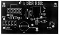
Guys, did you proceed with this issue? I have exactly the same problem. Thanks to this thread I found issue with ground plane connection Cin - IC GND went through vias and it was not enough low impedance connection. When soldered extra wire then Vout increased but not to supposed level.
I still could see irregular switching cycles at 260kHz, correct-spike-spike-correct. Cycles were dependand on resistive load 5r6-1r4. The only solution to get it working is hack with capacitor across diode. Even temporary capacitor to start function is enough when I remove it later then continues to delivery power. When inspecting V_switch then I see different wave forms after every power cycle. Sometimes nice regular equal rectangles, sometimes rectangles with alternating width when likely area of active period is equal to area in regular care in particular time. But the output voltage is stable and at supposed level 5V1. I see high-freq oscillation 78MHz in output voltage with high amplitude about 1-1.8V after switch. What LC circuit has influence on it?
I suspect "cycling issue" might be related to sensing max. current when some spike is detected as overcurrent and IC switches off FET. Feedback voltage seems stable - on the other side 78MHz oscillations should be there too but I cannot see anything dramatic. Also in block scheme is a RC which likely integrates feedback to remove spikes. I do not see more option how to tune it. Softstart is likely acting after power cycle only.
Mod: Link to old thread.
https://forum.allaboutcircuits.com/...ble-to-reach-full-voltage.159369/post-1387494
Last edited by a moderator: