Buck Converter Prototype

Thread Starter

Papabravo

Joined Feb 24, 2006
21,228
I recently discovered Power Electronics, by Daniel W. Hart as a free download from:

https://civildatas.com/download/power-electronics-by-daniel-hart and other sources

This book was published in 2014, so it is not a new work. I was drawn to the writing style and the examples that are presented in the text. In addition to covering the basic topology of many different SMPS types there is an emphasis on component selection. As an exercise in collaboration, I want to show the power stage for a buck converter and use it as a springboard for the staged development of a working converter.
1664999548907.png
This exercise shows a typical power stage for a buck converter along with the selection of the inductor and the capacitor. The simulation results show a pretty good match with the calculated values. I'm not entirely sure what the next step should be, but will doubtless include but not be limited to:
  1. Selection of a MOSFET switch
  2. Characterize the open loop response
  3. Decide on a control strategy
  4. Characterize the closed loop response
  5. Implement a loop compensation strategy
  6. Ensure an orderly startup phase
  7. Ensure stable and predictable operation
 

Attachments

eetech00

Joined Jun 8, 2013
3,961
Hi

So you have the frequency, DC, Vin, Vout, Iout, and ripple.
Next decide on operating mode, Voltage mode or Current mode, then choose a controller with and without an internal switch that supports your design spec and includes any extra features you may want (like shutdown or enable). Of course, cost should be considered. Since the output current is only 1A, the should be many devices to choose from. One that comes to mind is the LM2596 (but 150Khz). Also, in general, the higher the switching frequency, the smaller the inductor. Does the frequency have to be 20Khz? Or is that flexible? You see there will be trade-offs.

Hope I didn't misinterpret your post.
 

Thread Starter

Papabravo

Joined Feb 24, 2006
21,228
Hi

So you have the frequency, DC, Vin, Vout, Iout, and ripple.
Next decide on operating mode, Voltage mode or Current mode, then choose a controller with and without an internal switch that supports your design spec and includes any extra features you may want (like shutdown or enable). Of course, cost should be considered. Since the output current is only 1A, the should be many devices to choose from. One that comes to mind is the LM2596 (but 150Khz). Also, in general, the higher the switching frequency, the smaller the inductor. Does the frequency have to be 20Khz? Or is that flexible? You see there will be trade-offs.

Hope I didn't misinterpret your post.
None of the choices are fixed. The problem was taken from the mentioned text, as an example to show how to pick the inductor and the main filter capacitor from a set of specifications. We can change anything, but we are a long way from picking a chip because I want to examine the pieces inside the chip via simulation to promote understanding of the power conversion process.

Some of the choices in the problem may be less than practical. A possible contribution would be to offer a revised set of specifications for a more practical starting point for a device that would go beyond the simulation phase. There was a long-lasting thread on an EHT Power Supply if I recall correctly.

https://forum.allaboutcircuits.com/threads/eht-power-supply-design-and-construction.113504/

That thread has 2,146 posts so far. I should live so long.
 
Last edited:

Thread Starter

Papabravo

Joined Feb 24, 2006
21,228
So, I went looking for an external MOSFET switch by looking at the array of simulation models in LTspice and I started with a device that had:

\( V_{(BR)DSS}\;=\; 100 \text { V} \)
\( R_{DS(on)}\;\le\; 2\text{ m}\Omega \)

1665029633013.png

I found the IPT015N10N5ATMA1 at Digi-Key for the heartburn price of $8.14 for Quantity 1. How may in stock you ask? (You didn't really need to ask). Goose Egg, Nada, Zero. I suppose I could try to find a part in stock but by the time I need it who knows what the availability will be.

Would you now go for a device you can get, but may not have a simulation model or would go through the list of simulation models you have looking for one in stock?

Just an everyday engineering conundrum.
 
Last edited:

Thread Starter

Papabravo

Joined Feb 24, 2006
21,228
Why a 300A part when only a 3A part is needed?
I was only looking at Rds(on). It is actually somewhat difficult to select a part if you can't look at more than one thing at a time after the list has been sorted for all the parts with B(BR)DSS = 100 V. What 3A part did you have in mind?
 

eetech00

Joined Jun 8, 2013
3,961
I was only looking at Rds(on). It is actually somewhat difficult to select a part if you can't look at more than one thing at a time after the list has been sorted for all the parts with B(BR)DSS = 100 V. What 3A part did you have in mind?
Depends on the peak switching current supported by the controller.
 

Thread Starter

Papabravo

Joined Feb 24, 2006
21,228
So, I decided to search Digi-key for an N-channel MOSFET, with a V(BR)DSS of 100V and a maximum drain current of 3 to 3.3 Amperes that was in stock and less than $2.00 in single quantity. I found the FDT86106LZ from Onsemi.
https://www.onsemi.com/pdf/datasheet/fdt86106lz-d.pdf
Digi-key has 27,686 in stock @ $1.48 in single quantities.

Is there a simulation model -- you ask? Not with the standard LTspice distribution, and not in the extensive libraries of @Bordodynov but there is a pspice model on the Onsemi website, which I was able to use with LTspice without incident or incompatibility. This is a fairly common occurrence, but there are some exceptions.

The initial simulation results look OK for now and the switch losses at 1 A amount to 108 milliwatts at the maximum rDS(on).

1665073742040.png
 

Attachments

Thread Starter

Papabravo

Joined Feb 24, 2006
21,228
I tried really hard to characterize the open loop response of the prototype buck converter from the original problem in the book on Power Electronics by Daniel W. Hart which I mentioned in Post #1. It turns out that the open loop response at the low switching frequency is quite difficult to get a handle on because of the low switching frequency and the required values of the inductor and the capacitor. Raising the switching frequency to 100kHz and recomputing the values of L1 & C1 helps to make the open loop response more manageable. The MOSFET I introduced in post #8 seems to be just fine for this application.

1665113534678.png
 

Attachments

Thread Starter

Papabravo

Joined Feb 24, 2006
21,228
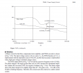
So here is the first shot at doing the open loop response of the 50V to 20V, 20 Watt Buck converter

1665251131910.png
I'm not entirely sure why things at low frequency appear to be so squirrelly. The peak between 2K & 3K is a bit of a surprise. The gain rolloff is much steeper than I expected, but I think I know why that is the case.
 

Attachments

qasdxx

Joined May 7, 2022
1
So here is the first shot at doing the open loop response of the 50V to 20V, 20 Watt Buck converter

View attachment 277989
I'm not entirely sure why things at low frequency appear to be so squirrelly. The peak between 2K & 3K is a bit of a surprise. The gain rolloff is much steeper than I expected, but I think I know why that is the case.
Why are you measuring the open loop response like that? In Hart he seems to be able to measure the open loop response by simply cascading the output LC filter, the 1/Vp PWM transfer function, and the error amplifier.

1697125683053.png1697125724338.png
 

Thread Starter

Papabravo

Joined Feb 24, 2006
21,228
Why are you measuring the open loop response like that? In Hart he seems to be able to measure the open loop response by simply cascading the output LC filter, the 1/Vp PWM transfer function, and the error amplifier.

View attachment 304755View attachment 304756
It is from the LTspice Help File under the "Method of Middlebrook"

How to get a Bode Plot from a SMPS


Parent Previous Next


Extracting Switch Mode Power Supply Loop Gain in
Simulation and Why You Usually Don't Need To
In the interest of stability, the open loop gain of a negative feedback system operating in closed loop should fall below unity with increasing frequency before too much phase shift occurs unless your aim actually is to make an oscillator[1]. This idea can be applied to the stability analysis of a Switch Mode Power Supply(SMPS). Even though a SMPS is an intrinsically non-linear circuit with no small-signal linear equivalent circuit, there typically is an analog feedback loop operating on the filtered, switched output.
There are two issues involved in determining the loop gain of a SMPS (i) obtaining the open loop gain from the closed loop system and (ii) ignoring the switching waveform by averaging over a switching cycle and/or using Fourier analysis to ignore the switching frequency components. The first issue is common to most stability analysis of feedback loops. Stability analysis is based on the open loop response but if you break the feedback loop to measure open loop response directly, the circuit doesn't work anymore which was why feedback was used in the first place. The second issue arises from the fact that a SMPS is an intrinsically non-linear circuit and linear feedback theory is basically restricted to small perturbations of a hypothetical waveform averaged over multiple switching cycles.
Determining the open loop response of a linear, closed loop system is a problem solved well by Middlebrook's method[2]. That method uses test signals injected into the closed loop system to independently solve for the voltage and current gains. These two gains are then convoluted together to get the true loop gain. If a point in the feedback loop can be identified where a low impedance drives a high impedance, then the current gain is zero and it is sufficient to measure only the voltage gain and identify that as the loop gain. Such a point can normally be found in a SMPS since you have a power supply output driving an error amplifier input.
Laboratory measurement of a SMPS loop gain is automated with commercial instrumentation pioneered by Venable Corporation and now also available from other companies. The technique of using injected test signals and Fourier analysis is called Frequency Response Analysis(FRA). While this method is routine in the lab, not everyone is aware of how to use it simulation. This article explains how to do FRA in LTspice XVII. The method uses the voltage gain part of the Middlebrook method, .measure statements to do the Fourier transform, a step statement to sweep frequency, and the feature in LTspice that allows one to plot the results of .measure statements. In reading through the steps below, you might want to refer to the working FRA examples that are part of the general LTspice XVII release typically installed in directory
%HOMEPATH%\Documents\LTspiceXVII\examples\Educational\FRA\
Step 1: Identify a point in the SMPS feed back loop where a low impedance source is driving a high impedance input. Two places are useful for this, either in series with the feedback pin of the SMPS controller or between the output to the top of the resistor divider going to the feedback pin.
Step 2: Insert a voltage source here. This will be a time-domain sine wave that perturbs the feedback loop. Give it a value of "SINE(0 10m {Freq})" The choice of amplitude(here 10mV) will impact accuracy and the signal to noise of the method. The smaller the amplitude, the lower the signal to noise. But if the amplitude is too large, the system is not operating linearly and frequency response becomes less relevant since the frequencies are no longer independent.
Step 3: Label the nodes to either end of this voltage source "A" and "B" The direction of feedback should be from node A to node B. For example, if the voltage source is connected directly to the feedback pin, node B is the feedback pin and node A is the one on the other side of the voltage source.
Step 4: Paste the following .measure statements on the schematic as a SPICE directive:
.meas Aavg avg V(a)
.meas Bavg avg V(b)
.meas Are avg (V(a)-Aavg)*cos(360*time*Freq)
.meas Aim avg -(V(a)-Aavg)*sin(360*time*Freq)
.meas Bre avg (V(b)-Bavg)*cos(360*time*Freq)
.meas Bim avg -(V(b)-Bavg)*sin(360*time*Freq)
.meas GainMag param 20*log10(hypot(Are,Aim)/hypot(Bre,Bim))
.meas GainPhi param mod(atan2(Aim,Are)-atan2(Bim,Bre)+180,360)-180
These .measure statements perform the Fourier transform of nodes A and B and then compute the ratio of the resultant complex voltages. The result is the complex open loop gain of the system. The magnitude is given by GainMag in dB and phase as GainPhi in degrees.
Step 5: Paste the following on the simulation command on the schematic as a SPICE directive:
.param t0=.2m
.tran 0 {t0+10/freq} {t0}
Parameter t0 is the length of time required for the system to come to steady state. You will probably have to run a few simulations to determine an appropriate value for t0. It occurs as the third parameter on the .tran command, meaning is it the time the simulator should start saving data. This prevents the .meas statements of Step 4 from using this data in the analysis. This is done because initial transient conditions might not be operating within the small perturbations from regulation that could be considered small signal response.
Notice that t0 appears in both the 2nd and 3rd parameters of the .tran command. The 2nd parameter is the stop time. The difference between start and stop times has been chosen as 10/freq, i.e., an integral number of perturbation cycles. Ideally, the Fourier analysis would be done over a period that is both an integral number of perturbation cycles and switching cycles, but his isn't always possible. Since loop gain must drop to less than unity at a frequency that is a fraction of the switching frequency, there are always more switching cycles than perturbation cycles and an integral number of perturbation cycles is used with the hope the error from a non-integral number of switching cycles will be small since many switching cycles are included.
Step 6: Choose which frequency or frequencies at which to perform the analysis. To do a single frequency, simply add this SPICE directive:
.param Freq=15K
and run the simulation. The output of the .meas statements are in the error log which you can view after running the simulation with menu command View=>SPICE Error Log. You can run the simulation at multiple frequencies by placing the following SPICE directive on the schematic:
.step oct param freq 50K 100K 5
This directive tells LTspice to run the simulation at frequencies from 50kHz to 100kHz using 5 points per octave. To plot this as a Bode plot, after the simulations complete, execute menu command View=>SPICE Error Log and then right click menu "Plot .step'ed .meas data" At this point, the Bode plot will not have any data plotted. so right click again and execute menu command "Visible Traces" and then select gain.
Armed with the above technique, one might feel ready to go and conquer SMPS design with Bode analysis of the feedback loop. I understand the temptation. It'd be rewarding if one could traverse the feedback loop identifying the components that gave rise to the poles and zeros, strategize which zeros to move to cancel which poles, and synthesize component values for the compensation network components to achieve a stable feedback loop. But that's pretty much exactly what you can't do with this technique or any other frequency domain technique for a current mode SMPS. Let me explain why.
Let's consider a typical fixed-frequency, peak-current mode switcher such as that in
%HOMEPATH%\Documents\LTspiceXVII\examples\Educational\FRA\Eg3.asc
The controller uses a flip-flop which is set by a clock pulse and turns on the switch which ramps the inductor current up. Once the peak switch current is proportional to the voltage on the output of the error amplifier, the flip-flop is reset, the switch turns off and the controller sits idle until the next clock pulse sets the flip-flop again. Since average current is proportional to peak current up to a geometrical factor, if we average over one clock cycle this flip-flop controlled-switch behaves like a transconductance. That is the current through the switch is proportional to the voltage on the output of the error amplifier. Now if we continue on along the feedback path, we have the inductor in series with the switch current. Since the switch is a current source, the series impedance of the inductor, even though it is reactive, causes no phase shift. This is actually the point to current-mode control and why you buy that controller. Continuing on the feedback path, we are now at the output of the SMPS. The output filter capacitor(C4) gives rise to one pole. The output is then divided by the feedback resistive divider and compared to a reference voltage at the feedback pin. The difference between the divided output and the reference voltage is the error voltage. This error voltage is amplified the the error amplifier to be a current which flows out of the error amplifier. But it is the voltage on the output of the error amplifier and not the current flowing out of it that determines switch current so to complete traversing the feedback loop, we need to convert that current to a voltage. We could do that with a resistor and that would work, but a much better idea is to use a capacitor(C1) because that will maximize the open loop DC gain to keep the output regulated to a stiff voltage. That capacitor makes a second pole.
Now, since each pole can cause a phase shift infinitesimally close to 90° and the controller must cause some additional delay, one might think that some circuit design is necessary to ensure a stable feedback loop. But that's not really the case because the output filter capacitor has ESR and that will put a zero in the response. Also, since we buy compensation cap C1 a series resistor, R1, that also puts another zero in the response. Further, the delay from the controller is a small fraction of the switching frequency. At the loop crossover frequency, which must be well below the Nyquist Frequency or half the switching frequency, that delay is in practise negligible. This means that the loop is stable and it isn't possible to synthesize component values since the loop is stable for all component values. This argument is basically pointing out that as soon as it is possible to describe the SMPS in the frequency domain, there are no stability problems, i.e., that the frequency domain is not an effect way to analysis a SMPS.
By and large, I find it pretty hard to make a current-mode SMPS unstable. For example, if you use an inductance value that is too high by an order of magnitude or two, then inductor ripple current becomes very small and the spoofed current of the slope compensation controls the flip-flop reset. That will reduce the impedance of the switched source driving this inductance to the impedance of the MOSFET Rds(on) plus the input source impedance so the inductor creates another pole in the loop and that causes instability. But in that situation, even though you're using a current mode controller, the power supply is actually running in voltage mode. Small signal linear analysis of voltage mode power supplies is quite useful because unless the feedback loop has been contrived to cancel one of the poles, the power supply will oscillate and may blow itself up the first time it is turned on. Current-mode supplies are quite different. While it is possible to do small-signal linear analysis of a current-mode switcher, there just isn't much engineering to be accomplished with the method since the feedback loop is stable as long as the power supply really is operating in current mode. If a current mode SMPS is unstable, it usually a high frequency issue that is averaged out of FRA/Bode analysis.
The last advice I can offer answers how one can be sure that a SMPS is stable and operating in current mode. The answer is to start with the schematic on the front page of the datasheet. The critical information there are the inductance value, output filter capacitance, and external compensation component values. Some datasheets give equations for computing these values, but I just start with those values and adjust using time domain simulation to evaluate the response. After all, the whole point of frequency domain analysis is to improve the time domain response. With current-mode switchers, it usually more direct to jump right to time-domain simulation to check overshoot since stability has already been achieved.
1] The discussion is restricted to minimum-phase systems.
2] R. David Middlebrook, "Measurement of Loop Gain in Feedback Systems", International Journal of Electronics (vol 38, no. 4, pages 485-512, April 1975).
Copyright © 1998-2022 by Analog Devices Inc.. All Rights Reserved.

This method may be unnecessary in LTspice (17.1.15) which has introduced new primitives for doing this kind of thing. Qspice has also implemented a "Bode" analysis in transient mode. Check the Qspice help files and Demo files for details.
 
Top