Breakout Box Help

Thread Starter

bwilliams60

Joined Nov 18, 2012
1,442
Hey all, hope everyone is staying safe and healthy.
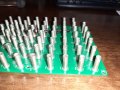
I am trying to build a breakout box and I have two questions.
1) What do You call the tubes that are roughly 3/4" long that solder to a PCB and allows you to plug In banana jack probes. I have seen them used in DVOMs as well.
2) How do you represent these with a symbol in Kicad or EASYEDA?
I am just running a DB connector, through a trace to the posts soldered to a PCB board.
Any help appreciated.
 

Thread Starter

bwilliams60

Joined Nov 18, 2012
1,442
I believe they are called pin receptacles. Now I just need to know how to show them on a KICAD schematic. Single connector?
 

Thread Starter

bwilliams60

Joined Nov 18, 2012
1,442
Hey @Alec_t, that is close but what I am really after is the symbol I would use in KiCAD to represent these or at least the hole that they would sit in. I am not too familiar with PCB design and learning as I go so I am wondering if I use a single point connector symbol or something else? Still looking for 62 pin D-Sub symbol as well for KiCAD,
 

hrs

Joined Jun 13, 2014
394
Hi,

On the schematic I would use Conn_01x01_Female for this, see screenshot below. Then for the footprint any single pad footprint would work, for example Banana_Jack_1Pin. Then on the PCB layout you can right-click the pad and choose properties (or hover over the pad and press E) and set Size X and Hole size X to what matches your physical hardware. Finally, when you've set the pad to what you want, you can right click that pad again, choose pads -> push pad properties which will allow you to set other footprints to the same dimensions as this one.

Edit: In the standard symbol library there is no 62 pin D-Sub. But you could copy and modify DB37_male or _female and add however many pins you need, ie. make your own symbol (and footprint).
conn_01x01_Female.png
footprint.png
pad_properties.png
 
Last edited:

Thread Starter

bwilliams60

Joined Nov 18, 2012
1,442
@hrs, that is some solid material there. Thank you for the great answer. I am going to work on the symbol tonight. Not sure how to expand a DB37 but I am sure I will figure it out. I have gotten to the finish line a couple of times in KiCAD but I don't use it enough to remember everything so I have to relearn as I go. Thank you again.
Any idea how to make the solid pin representation in this diagram?
1591587718286.png
 
Last edited:

hrs

Joined Jun 13, 2014
394
Hi bwilliams,

Have a look here for how to make symbols and footprints:

Below is a screenshot of a deconstructed DB15. The solid pins appear to be circles with a fill. I added a bigger one to test. Note that to select a circle you need to click it on the very edge or nothing will happen.

dsub.png
 

Thread Starter

bwilliams60

Joined Nov 18, 2012
1,442
Do the dimensions etc of the schematic symbol have any importance or is that only an issue when you make your footprint. Also, does orientation of the pins matter at this point? So do I need to put Pin #1 in bottom left, bottom right etc or does it matter?
 

hrs

Joined Jun 13, 2014
394
The bare minimum that you need is the correct number of pins. The numbering on the symbol will match the numbering on the footprint, so the symbol should be descriptive enough that you can see what you are connecting to in the schematic. Try it out and you will see.
 

Thread Starter

bwilliams60

Joined Nov 18, 2012
1,442
1591674793227.png
My dot seems to be much bigger than my connector.
How do I make it smaller or do I spread out my connections?
How do I make the line from the dot to the connection?
 
Last edited:

hrs

Joined Jun 13, 2014
394
I prefer to keep the discussion here because if I don't know the answer someone else can jump in and if I do know the answer it might help out more people.

All the program needs from the symbol is the correct number of pins. The rest like orientation and dimensions is fluf for humans. For the footprint orientation and dimensions are important to the program too.

To manipulate objects in the symbol editor you can use one of these 3 methods:
#1 - Drag a selection box around the objects you want to maniputlate; place your mouse pointer somewhere above and to the left of said object, press and hold left mouse button (LMB), drag the mouse pointer below and to the right of the objects, release LMB. Selected objects will now move with your mouse pointer. At this point you can also use E, R, Delete. E only works if a single object was selected. More below.
#2 - Right-click an object to make a context menu appear. Available options depend on the type of object. Objects can be picky where they are clickeable. If it's not working, try harder (try the edge)!
#3 - Place your mouse pointer over any object you want to manipulate. Press any of E, G, M, R, Delete ... maybe there are more. This will only work if that option is available for the object to be manipulated.

Options:
E - Edit object properties
G - Grab and drag an edge. For resizing circles, rectangles etc.
M - Move object(s)
R - Rotate object(s)
Delete - Delete object(s)

Grid size:
The reason your dot is as big as it is is probably due to the grid settings. You cannot draw shapes smaller than the grid spacing. In the main window of the symbol editor right-click anywhere on an empty space. You can set the grid in the context menu that appears. Or click View -> Grid settings.
 

Thread Starter

bwilliams60

Joined Nov 18, 2012
1,442
Okay I have what I think is a viable connector. What do I need to do to my diagram now? I have stopped short of connecting 62 wires with to questions.
1) Do I need to connect all 62 wires or is there a faster/neater way of doing it?
2) What about the overhang on the right side past the schematic border? What do I do about that?
1591714462107.png
 

hrs

Joined Jun 13, 2014
394
I don't know of any other way than to wire up all pins like you are doing now. Note that you can hide the "Conn_01x01_Female". It's not very informative here and takes up too much space. To do so, place your mouse over the text and press E, set visibility as desired. Then copy the pin 61 times (mouse over pin, press C). Or set visibility 61 more times.

I would move the pins such that only a horizontal wire is needed to connect it to the D-Sub.
dsub_schem.png
 

Thread Starter

bwilliams60

Joined Nov 18, 2012
1,442
Do I have to renumber them to match my 62 pin or my "J" configuration ie J1 = 1, J2 = 2 etc or does it matter?
Here is what I have now. I guess you can also attach pins and connectors with "labels"
1591729300963.png
 

hrs

Joined Jun 13, 2014
394
My inner autist wouldn't have it any other way but it's not required. The software doesn't care if the numbers match.
No need for labels here, but you can use them to give nice names to a net.

As you have it it's messier than it needs to be, but it will work.
 

Thread Starter

bwilliams60

Joined Nov 18, 2012
1,442
LOL. Clean up comes after I learn how to master this program. If that is possible. On to the next step whatever that may be. I guess I am transferring it to a PCB and setting up footprints.
 
Top