Facebook
 Google
 GitHub
 Linkedin
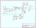
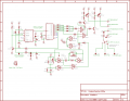
Added next segment. Replaced trimmers + resistors with single resistors (R12,R13) at about midway point ([(50k/2)+10k)] from Ken's original) Not sure how to get pin 14 on the 4098 to connect properly. Couldn't figure out how to get a "package' to display so could just connect the pins, & since unfamiliar with design technics in general, not sure if it's done with the gates as SOP anyway.
Attachments
-
 229.4 KB Views: 44