Board repair help, are all 555 times the same ???

Thread Starter

xtal_01

Joined May 1, 2016
227
Do not disassemble the board or remove any component. I have already drawn the circuit schematic. We should be able to apply voltage and check the functionality of the board.

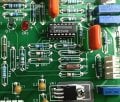
We need to identify the resistor values but I cannot be certain of the color bands from the photographs.
Write out the color bands you see. You can use abbreviations shown. All the resistors have 5-band codes, ±1% tolerance. (The 5th band is Br). Sometimes it is difficult to determine the order of the bands, left to right, or right to left. A resistance measurement would help to decide which is the correct value.

0 Bk
1 Br
2 R
3 O
4 Y
5 G
6 BL
7 V
8 Gy
9 W

https://resistorcolorcodecalc.com/

Not all values are possible. Resistor color bands should match values from the E96 series.

https://www.logwell.com/tech/components/resistor_values.html

Measure the resistance while in-circuit to give some estimate of the value. This measurement is not 100% accurate since you are measuring the resistance of all components connected in parallel with this resistor.

I have started a list below with some examples.

R1 - 5 kΩ trimpot CAL
R2 - 5 kΩ trimpot ZERO
R3 - 5 kΩ trimpot MAX
R4 - Ω
R5 - Ω
R6 - Ω
R7 - R Y W R Br = 24.9 kΩ
R8 - 49900 Ω
R9 - Ω
R10 - Ω
R11 - Ω
R12 - Ω
R13 - Ω
R14 - Br Bk R Br Br = 1.05 kΩ
R15 - Br Bk R Br Br = 1.05 kΩ
R16 - Ω
R17 - Ω
R18 - Ω
R19 - Ω
R20 - Ω
R21 - Ω
R22 - R Y W R Br = 24.9 kΩ
R23 - BL Bk Y Bk Br = 604 Ω
R24 - Ω
R25 - Ω


There are some markings visible on CR1 and CR2. Write down what you can see.
WOW ... you are fast! I worked on it all yesterday and last night and only got half way through. I am working on the values right now. Just FYI ... R2 is 1K (102 while the other two are 502 .... just looked them up).

You read my mind ... my first thought was how do you know which end to read from. I started double checking with my meter to make sure I got it right.

So far R8 is the only one that is way off. It looks a lot different than the other resistors. It has a number RN60D 4992F on it. If I am reading the sheet right, that means 49.9 K .... I am only reading 2.1 K ... but as you said, that might be because it is in circuit. I just pulled the chips out and rechecked the values ... wanted to make sure the chips are not changing the readings.

Great resistor calculator !!!!!!!!!! I am soooooo old, I still have my little Radio Shack one (cardboard with wheels) here somewhere.

I really appreciate this !!!!!!
 

MrChips

Joined Oct 2, 2009
34,984
What is connected to the left leg of R26?

It is strange that the trace at LM324 U1-3, wraps around R21 right leg and connects to R10 left leg.
Yet on the reverse side, R21 is connected to R10.

This is leading to a suspicion that someone gave you a board that never worked in the first place because of layout errors.

AAC_PCB_R26.jpg
 

Thread Starter

xtal_01

Joined May 1, 2016
227
What is connected to the left leg of R26?

It is strange that the trace at LM324 U1-3, wraps around R21 right leg and connects to R10 left leg.
Yet on the reverse side, R21 is connected to R10.

This is leading to a suspicion that someone gave you a board that never worked in the first place because of layout errors.

View attachment 339461
No traces on the bottom of the board.

On the top, the trace heads back under the resistor (R26) then T's into the trace between pin 6 of the IC and the right side of R10

Does that make sense?

I can draw a picture if it helps.

Thanks so much again!
 

bertus

Joined Apr 5, 2008
22,977
Hello,

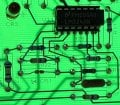
In post #12 there are some pictures with light shining though the board.
R26 has no connection.
R21 connects to R10.

IMG_0317_555_board_top_detail.JPEG

Bertus
 

Thread Starter

xtal_01

Joined May 1, 2016
227
Hello,

In post #12 there are some pictures with light shining though the board.
R26 has no connection.
R21 connects to R10.

View attachment 339471

Bertus
No traces on the bottom of the board.

On the top, the trace heads back under the resistor (R26) then T's into the trace between pin 6 of the IC and the right side of R10

Does that make sense?
 

Thread Starter

xtal_01

Joined May 1, 2016
227
Do not disassemble the board or remove any component. I have already drawn the circuit schematic. We should be able to apply voltage and check the functionality of the board.

We need to identify the resistor values but I cannot be certain of the color bands from the photographs.
Write out the color bands you see. You can use abbreviations shown. All the resistors have 5-band codes, ±1% tolerance. (The 5th band is Br). Sometimes it is difficult to determine the order of the bands, left to right, or right to left. A resistance measurement would help to decide which is the correct value.

0 Bk
1 Br
2 R
3 O
4 Y
5 G
6 BL
7 V
8 Gy
9 W

https://resistorcolorcodecalc.com/

Not all values are possible. Resistor color bands should match values from the E96 series.

https://www.logwell.com/tech/components/resistor_values.html

Measure the resistance while in-circuit to give some estimate of the value. This measurement is not 100% accurate since you are measuring the resistance of all components connected in parallel with this resistor.

I have started a list below with some examples.

R1 - 5 kΩ trimpot CAL
R2 - 1 kΩ trimpot ZERO
R3 - 5 kΩ trimpot MAX
R4 - Ω
R5 - Ω
R6 - Ω
R7 - R Y W R Br = 24.9 kΩ
R8 - 49900 Ω
R9 - Ω
R10 - Ω
R11 - Ω
R12 - Ω
R13 - Ω
R14 - Br Bk R Br Br = 1.05 kΩ
R15 - Br Bk R Br Br = 1.05 kΩ
R16 - Ω
R17 - Ω
R18 - Ω
R19 - Ω
R20 - Ω
R21 - Ω
R22 - R Y W R Br = 24.9 kΩ
R23 - BL Bk Y Bk Br = 604 Ω
R24 - Ω
R25 - Ω


There are some markings visible on CR1 and CR2. Write down what you can see.

Edit: Typo error on R2.
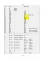
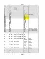
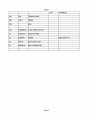
OK .... sorry I am soooo slow but I worked at it all afternoon and got a list. The only thing not on the list is the CR1 (a zener diode with 56A on it) ... CR2 (regular diode with 1n ???? on it ... the ??? numbers or on the bottom) ... and CR3 which is an LED. I measured each one with my meter as when identified them. I highlighted a couple that jumped out at me. Hope I read the caps right ... they were hard to get a good value for. So far the odd looking resistor seemed way off and also C3 ... but I an not sure as they are still in circuit.

Thanks!
PARTS_LIST.jpg
 

MrChips

Joined Oct 2, 2009
34,984
Trace from bottom leg of R20 disappears under U1 to ?.

U1-6 is connected to ?

U3-2 is connected to ? under U2.
Can you use the ohmeter and trace the two traces going under U2, and also two traces under U3?
 

Thread Starter

xtal_01

Joined May 1, 2016
227
Trace from bottom leg of R20 disappears under U1 to ?.

U1-6 is connected to ?

U3-2 is connected to ? under U2.
Can you use the ohmeter and trace the two traces going under U2, and also two traces under U3?
1) R20 goes to Pin 2 on IC U1... then continues ontoR22 and then CR1 and then R9

2) U3 pin 2 goes to U2 pin 8 (trace on the top) ... then U2 pin 1 continues underneath to U2 poin4 ... R19, then to pin4 of connector P2 .... plus, R19 on top (same end the lower trace hits) goes to R1 pin 3 ... then on the bottom from there a trace goes R4, R3 pin 3, C3 +, the regulator pin out, and R8

3) U2 ... Pin 1 goes to C7 and pin 7 of C1and the other way to r23, c8, c1 +c2 -, c3 -, Pin 5 of P5 and the center pin (ground) of the regulator ... which goes on to R3 pin 1, com on P4, R1 pin 1, c5, U1 pin 12

4) U3 ... pin 1 NC, pin 2 (see answer 2) ... pin 3 goes to R19 ....pin 4 NC .... pin 5 to pin 2 if P1 ... pin 6 goes to in 4 of P1 ... pin 7 NC and 8 goes to pin 1 of P1 and S1-B which goes to Q1 collector

WOW ... the transistor was fun. I am guessing it is obsolete. Non at Mouser or Digikey. Found a few on ebay ... panicked want I found data sheets but nothing in stock.

Anything else I need to check?

Thanks again so much !!!!!!!!!!
 

MrChips

Joined Oct 2, 2009
34,984
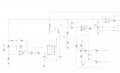
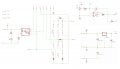
Here is what I have so far. Accuracy not guaranteed.
There are external voltages that are unknown. I have labeled these as +12V, -12V, and V+ for now.
+12V goes to U1-4.
-12V goes to U1-11.

Some connections have yet to be identified, namely, trace from R24-R25 node leading to under U2.
At this stage, the function of the circuit is still not identifiable. It would be very difficult to access the proper functioning of the board without knowing the specific application.

Higher magnification images can be provided.

PCB6_1A.jpg

PCB6_1B.jpg
 

Thread Starter

xtal_01

Joined May 1, 2016
227
Here is what I have so far. Accuracy not guaranteed.
There are external voltages that are unknown. I have labeled these as +12V, -12V, and V+ for now.
+12V goes to U1-4.
-12V goes to U1-11.

Some connections have yet to be identified, namely, trace from R24-R25 node leading to under U2.
At this stage, the function of the circuit is still not identifiable. It would be very difficult to access the proper functioning of the board without knowing the specific application.

Higher magnification images can be provided.

View attachment 339529

View attachment 339530
Incredible! Your wiring is very impressive! I will check that one trace. Should I go though it and double check the drawing vs the board or just come up with a plan to check individual components or ?

What program did you use for this ... really looks great!

Thanks again so very much !!!!!!!!!!
 

MrChips

Joined Oct 2, 2009
34,984
I would not go about any repair job by looking for a bad component. I would test for working functions. If you don't know what the board is supposed to do then the board should be given back as is to the client.

I used Eagle to reverse engineer the board. In terms of wiring checks, I would rebuild the PCB exactly as the original and then check for differences.

For functional tests, I would run the circuit through a simulator. It would surely help if we knew where the board came from and what it is supposed to do.
 

Thread Starter

xtal_01

Joined May 1, 2016
227
I would not go about any repair job by looking for a bad component. I would test for working functions. If you don't know what the board is supposed to do then the board should be given back as is to the client.

I used Eagle to reverse engineer the board. In terms of wiring checks, I would rebuild the PCB exactly as the original and then check for differences.

For functional tests, I would run the circuit through a simulator. It would surely help if we knew where the board came from and what it is supposed to do.
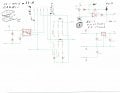
I don't know how you traced and drew it so fast. It took me two days to trace and then a day to compare your drawings with mine. I found a few corrections on mine ... made them.

There is a few things on your drawings I marked up. Can you take a look at them and double check me Your drawings will obviously be much easier to follow than mine when testing the board.

One question ... this board has three sealed pots. Can I assume if I do find the bad part and replace it, it would throw off the calibration? Or maybe replacing one part might not have a huge effect but just replacing all the parts on the board would?

Finally, I have attached the parts list with the values I got when measured in circuit. I highlighted a few that jumped out at me. Any "best guess" as to what part / parts failed?

Thanks so much !!!!!!!!!!!!!
board-Model_small.jpgCCI_000007.jpgCCI_000008.jpgPARTS_LIST-0001.jpgPARTS_LIST-0002.jpg
 

MrChips

Joined Oct 2, 2009
34,984
The three trim pots were adjusted and sealed on a test bench. Since we have no idea what the circuit does it would not be possible to adjust the trim pots to the required specifications.

You cannot go by the measured values of the components while they are still in circuit.

Even if you find a part that does not match the expected value, you still cannot verify that the board will be working when fresh components are installed.

I would return the board as not fixable.
 
Top