Facebook
 Google
 GitHub
 Linkedin
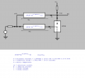
I've been trying to write a Python code that recreates the simulation of a simple NPN BJT in LTSpice, but i have been having difficulties on finding the exact equations they use in the software, i have stumble upon some equations that is used in the gummel poon model, but the results in the simulator never matches exacly on the code i create based in these equations. Does anyone know where i can find these equations ?
BJT LTSpice Gummel-poon Model
- Thread starter alexandre1908
- Start date