BJT common collector amplifier design.

LvW

Joined Jun 13, 2013
2,037
So I'm required to design a BJT common collector amplifier. We were told to use the circuit from the textbook (picture provided below). It has to have a current gain of 20.
Beta = 100
ic= 10mA
Vce= 1.0V
.......................
Does that mean all previous calculations are wrong?
Max, from the beginning I was not completely sure about your requirements (as repeated above). Are you?

* Beta=100 (exact) or at least 100?
* Vce=1 V (does your current design meet this requirement?)
* Ic=10 mA (I think you have about twice that value, don`t you?)
* No spec for the external load resistor?
* Are you allowed to deviate (by how many %) from the requirements?
........................
 

Thread Starter

Max Kreeger

Joined Oct 1, 2013
95
The specs that you quoted are direct from the transistor data sheet. They haven't specified how much we can deviate. I'm still confused about these external values. What exactly is external resistance.
 
Last edited:
When I did the calculations along with efron using 100 as beta..we got a gain of 20 spot on. So how did it change?
Does that mean all previous calculations are wrong?
What I was trying to point out is that the mathematical calculations made by hand may not (and probably don't) compare to the results of the LT spice simulations because the β used in the simulations comes from the 2N3904 model used by LT spice, and it probably isn't 100. The 2N3904 model β can probably be changed to be exactly 100, but I don't think you and Efron did that.

This means that unless you change the LT spice 2N3904 model β to be 100, you can't use LT spice to design a circuit to meet the current gain requirement.

One could find out the effective β used by LT spice by probing the AC base current and the AC collector current.
 
Last edited:
This circuit has no feedback mechanism to stabilize the current gain. The voltage gain is stabilized by feedback, but not the current gain.

Two main features of this circuit (besides β) determine the current gain.

At the input, the applied signal current divides between Rb and Zit; only some of the signal current actually enters the base of the transistor.

At the output, the output current from the transistor divides between RE and RL; only some of the current makes it to RL.

If you were to use the circuit in figure (a) of the first image in post #1, not changing RE or RL, but changing β to 100, you could achieve a current gain of 20 by just changing R1 and R2 (keeping them equal to each other). This would change the fraction of the input signal current that reaches the transistor base, and that would change the overall current gain of the circuit.
 
The specs that you quoted are direct from the transistor data sheet. They haven't specified how much we can deviate. I'm still confused about these external values. What exactly is external resistance.
The external load resistor is RL.

When you say that the specs quoted are direct from the transistor data sheet, apparently that means that they are not a part of the problem requirement.

You said that you are supposed to use the circuit in the attachment. Maybe that means you should leave β at 200, as shown in the attachment.

Perhaps you are supposed to realize that adjusting R1 and R2 can change the overall current gain, and achieve an Ai of 20 by that means.

You could also vary Ai by changing RL and leaving R1 and R2 alone.

You might ask the instructor for clarification.
 

Thread Starter

Max Kreeger

Joined Oct 1, 2013
95
Current gain is given has to be 20. DC voltage is selected. Those specs are from the data sheet from the transistor I used in LTspice. Its the same transistor I used in real life. So I got to stick with the specs of beta is 100 etc. We can use any diagram to design ours the lecturer just helped us out by providing one. We didn't have to use it. We're supposed to get the gain by any means necessary.
 
Current gain is given has to be 20. DC voltage is selected. Those specs are from the data sheet from the transistor I used in LTspice. Its the same transistor I used in real life. So I got to stick with the specs of beta is 100 etc. We can use any diagram to design ours the lecturer just helped us out by providing one. We didn't have to use it. We're supposed to get the gain by any means necessary.
Do you understand that in real life, the transistor you use is unlikely to have a β of exactly 100?

If you build this circuit and use a transistor with a β of something other than 100, the overall circuit gain will not match your calculations when those calculations are done with a β of 100.

Did you find your specs here:

http://2n3904.com/

They even have an example circuit like yours!

If you consult a complete data sheet:

http://www.fairchildsemi.com/ds/2N/2N3904.pdf

you will see that the minimum (at Ic=10mA) DC HFE is 100. This means that the typical 2N3904 will have a larger current gain. A value of 200 might be typical.

Are you expected to go into the lab and show that your real circuit has a current gain matching your mathematical design? If so, then you better measure the hfe of your actual transistor and use that value in your calculations.
 

LvW

Joined Jun 13, 2013
2,037
............
We can use any diagram to design ours the lecturer just helped us out by providing one. We didn't have to use it. We're supposed to get the gain by any means necessary.
Does this mean you are NOT required to have a current gain of 20 with regard to an external load resistor (connected via C with Remitter) ?

Are you even free to select another dc biasing scheme?

(You see, it would be much easier for us to help you and to discuss with you if you had given us from the beginning a COMPLETE description of the task).
 

Thread Starter

Max Kreeger

Joined Oct 1, 2013
95
The Electrician, that second data sheet you posted is the one I used, and yes I'm required to demonstrate it working in the lab so it matches my calculations - I've think I've got enough information here to go back and re-work through my calculations. Thank you! :)

LvW: I didn't think it was so complex to describe, a value goes in... a gain of 20 comes out. Yes we are free to use another scheme, but I was already provided with one so stuck with it.
 

LvW

Joined Jun 13, 2013
2,037
LvW: I didn't think it was so complex to describe, a value goes in... a gain of 20 comes out. Yes we are free to use another scheme, but I was already provided with one so stuck with it.
OK - let me answer with one general statement:
*If you are analyzing a given circuit there is only one single solution.
*In contrary, if you have the task to DESIGN a circuit to fulfill a certain specification there is, in principle, a number of infinite solutions.

Therefore, it is important to know these requirements as well as some boundary conditions (if any).

With regard to your task - at least to me - it was not clear from the beginning
- if you are free to select a certain circuit configuration,
- if the power supply is given,
- if you have to consider a particular beta value of 100
- if you are required to allocate the given curent gain to an external load resistor or to the emitter resitor only.

Please consider this answer not as a kind of accusation (charge) but rather as an attempt to help you how to describe a certain technical project in a clear and unambigious manner.
 

Thread Starter

Max Kreeger

Joined Oct 1, 2013
95
LvW: Sorry, it was my first time ever designing a circuit and when I started I didn't fully understand the concept. Didn't realise how important initial conditions were.

Had a talk with lecturers. They were pretty lenient with the gains, as long as it was around 20 they were happy.

Continuing on though I tested both my emitter and collector amps. Emitter has a gain of ~18 and the collector seems to be working. Just want to confirm though for demonstrating the current gain. Can I use the calculation of Ai = Zi/RL...would that be sufficient?? Only other method I can think off is to run a multimeter in series with the circuit but that means breaking it.
 

Attachments

Efron

Joined Oct 10, 2010
81
Just want to confirm though for demonstrating the current gain. Can I use the calculation of Ai = Zi/RL...would that be sufficient?? Only other method I can think off is to run a multimeter in series with the circuit but that means breaking it.
Max,

For the output current, as you know RL and it's fixed value, you can deduce Iout with Ohms law from voltage drop there.

For the input current, it would be nice to have a current source in your lab. Have you one?

You can insert a multimeter between the input voltage source and your input capacitor. However, if the current here is supposed to be low (e.g. micro-amp) it will be difficult to have practical measurement. A best practice in this case is to add a well known small value resistor, let's say 1ohm for example, instead of the multimeter. Then measure the voltage drop in this resistor with the oscilloscope.

To facilitate the reading at oscilloscope, you could go for higher values, e.g. 10ohms or even 100ohms to measure the current (this is OK as long as you know what you're doing and where in your circuit). Obviously this resistor will be seen as a power loss by the input voltage source. However, the current gain between the input pin of your amplifier and the output will remain the same because you're being intrusive but before your input pin (in this context you're intrusive in voltage gain because you add a resistor in series with the voltage source. However, for the demonstration of current gain, it is OK).

There may be other suggestions out there.
 

LvW

Joined Jun 13, 2013
2,037
Continuing on though I tested both my emitter and collector amps. Emitter has a gain of ~18 and the collector seems to be working. Just want to confirm though for demonstrating the current gain. Can I use the calculation of Ai = Zi/RL...would that be sufficient?? Only other method I can think off is to run a multimeter in series with the circuit but that means breaking it.
* It is the first time I hear that you also are designing a common emitter stage.
* Ai=Ri/RL is for calculation purposes. Of course, you should verify it by measurements.
Please note that a multimeter in current mode does not "break" the circuit. But don`t forget: You have to measure currents in the kHz range.
 
Last edited:

Thread Starter

Max Kreeger

Joined Oct 1, 2013
95
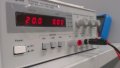
Efron: We do have a current source, but we were never told to actually set it to anything. Only to use the voltage side of things as you can see in the picture. Now this confuses me "you can deduce Iout with Ohms law from voltage drop there." ...would I be using the 20V? or the 1Vpp? or the actual measured pk-pk of 920mV?? I'm guessing the 20V to get 0.02? Is that what you mean?

LvW: Yeah I was supposed to design an emitter and collector but only needed help with the collector side of things as you can see.. haha

Once again guys I'm sorry for my repetitive questions. I've learnt more from you guys than my lectures. Thank you again for your patience.
 

Attachments

Efron

Joined Oct 10, 2010
81
Efron: We do have a current source, but we were never told to actually set it to anything. Only to use the voltage side of things as you can see in the picture. Now this confuses me "you can deduce Iout with Ohms law from voltage drop there." ...would I be using the 20V? or the 1Vpp? or the actual measured pk-pk of 920mV?? I'm guessing the 20V to get 0.02? Is that what you mean?
Max,

Keep concentrate on your objective. You're looking for the current gain, isn't it? So, you need to somehow measure Ai = Iout/Iin.

Because of the coupling capacitors, you only need to measure ac signal.

As you cannot directly measure currents with the oscilloscope, you must measure voltages and deduce currents from those measures.

Iout = Vout/RL and you measure Vout with the oscilloscope over RL - I think it was 920mVpp right? Well, this is not the value you'll use >> demonstration coming soon ...

For Iin, I would use the resistor in series with the voltage source (see my previous post) as you cannot use the current source (why they don't let you use it for a current amplifier demonstration :mad:).

You measure the voltage drop in that resistor so that you can calculate Iin = Vresistor/Rresistor (make a schematic and you'll better understand why this current is Iin)

Because you're adding a resistor to your input, the final current going through the amplifier will be different that the proper one without that resistor. This is the reason why the 920mVpp you got at the output (over RL) cannot be used with the new configuration. You have to measure it again.

So, to sum up, you add a resistor just after your input voltage source , and you measure the voltage drop on RL and Rresistor.

Then you have

Ai = Iout/Iin = (Vout / RL) / (Vresistor / Rresistor) =
= (Vout * Rresistor) / (Vresistor * RL)

Be careful with the units (e.g. don't mix up mA with uA)

I hope it is clear now.
 

Thread Starter

Max Kreeger

Joined Oct 1, 2013
95
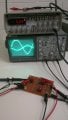
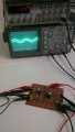
Ok, I added the 50ohm resistor in and got these results.. Ill try test again with the more accurate equipment.


EDIT:
Went back and swapped the resistor to 10K like in the original design and got this result: Input is 1V output is 0.7. So by your formula Ai = Iout/Iin = (Vout / RL) / (Vresistor / Rresistor) =
= (Vout * Rresistor) / (Vresistor * RL)

My Vout and the voltage across the 10K resisitor were both 0.7V

0.7 * 10K = 7000
0.7 * 1K = 700

So thats a gain of 10??

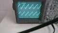
Don't know why signals messed up..tested on another machine and it was fine. Same values though.
 

Attachments

Last edited:

Efron

Joined Oct 10, 2010
81
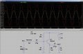
I suppose you're using the schematic given hereafter. Please confirm !

Using LTspice everything is correct using both 50ohms or 10K for Rresistor (red signal is Vout at RL and green is voltage drop through Rresistor).

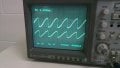
First thing to start with: In the oscilloscope, the wave form at the Rresistor and RL should be both sinusoidal and it is not the case. Why? Are you still using sinusoidal input source? A reader could think you're using a ramp input signal instead.

Also confirm the input voltage, is it still 0.5V amplitude (=1Vpp)?

This is important; The gain of 20 is only valid if the transistor is working in its linear region, that is, without distortion. If you're introducing a sinusoidal signal and you don't see sinus in the oscilloscope, there is distortion (for some reason) and the calculations are no more valid.

The fact that you introduce a serial resistor at input must not introduce signal distortion to the circuit because a resistor has linear behavior. If the signal at VB was sinus before, it must still be be the case after adding Rresistor.
 

Attachments

Last edited:

Thread Starter

Max Kreeger

Joined Oct 1, 2013
95
It is sinuisoidal (the machines just a bit out of whack) I tested on another machine and it was a perfect sine wave, but like I said I got the same values. Only reason I switched to 10K is because I couldn't really see a difference. Unfortunalty I can't use the digital equipment to get a more accurate reading.

So according to your simulaion its a gain of 31.8?

I understand what you're doing. Makes sense. I'll just wait until I can get on the digital equipment and get direct readings.
 

Efron

Joined Oct 10, 2010
81
My simulation give me a current gain of 23.33 = (0.7/1K) / (0.3/10K).

OK, maybe this can help,

Take the measures separately, one channel at a time. Only connect two leads of the oscilloscope at a time.

I have a feeling about what's going on but not sure of that.
 
Top