Biasing is done with the resistors, not with the capacitors. The resistors in each circuit are the same.
The base in each circuit has a high impedance and the emitters have a low impedance that needs the larger capacitor in both circuits.
Biasing is done with the resistors, not with the capacitors. The resistors in each circuit are the same.
The base in each circuit has a high impedance and the emitters have a low impedance that needs the larger capacitor in both circuits.
Thanks for clarification
Sure , capacitors aren't a part of the biasing , I meant to say , is it necessary to changing the capacitors with changing the circuit?
For the MW band , are capacitors mentioned in the CB circuit accurate ?
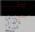
Your biasing caused the severe clipping at the top of the waveform. I changed the biasing a little and reduced the input signal level to reduce the clipping. It is still distorted because it is missing some negative feedback.
Your biasing caused the severe clipping at the top of the waveform. I changed the biasing a little and reduced the input signal level to reduce the clipping. It is still distorted because it is missing some negative feedback.
I was wondering , is there are a differences in biasing between CB & CE circuits
I thought of , as long as the signal will be input into the emitter ,then its resistor should be as high as possible
to avoid weakening the signal , which will be pass in the emitter's resistor to the battery (-) line as well .
A common base transistor amplifier transistor has a very low input impedance then stray capacitance at the input does not attenuate very high frequency signals.
If you increase the resistance of the emitter resistor then you must also increase the resistance of the collector resistor so that the biasing is not completely messed up.
Here is the frequency response of the common emitter amplifier I corrected: I deleted the incorrect amount of gain. See my next post.
thanks for your concern
That's OK , but the circuit is common emitter , my goal is the common base circuit
plus , no resistor at the collector , there is a RF transformer .
I have never designed or simulated a common base transistor with a transformer at the collector.
I noticed that the emitter input capacitor value must be about double the value of a common emitter capacitor value for the same low frequency cutoff.
well spotted and that was incorrect or at best incomplete.
instead of "base is always an input" should be "base cannot be an output" since only input current ever flows through it. so when base is 'fixed' (as in common base case), then the only way to affect or control the input is to change biasing at emitter. since current in emitter circuit is large (much larger than input current), impedance at that point is low.
Yes - and to be more clear - "biasing at emitter" should mean: Set resp. modify the bias VOLTAGE at the emitter (when the base is DC grounded) because it is the base-emitter voltage that matters. The currents are the result of the voltages Vbe resp. Vce.
 Facebook
 Google
 GitHub
 Linkedin