Facebook
 Google
 GitHub
 Linkedin
Hi all.
I am very new with this (Usually using standard breadboard MCUs).
There was a question in my mind if I can build my own boards for a project at home.
Essentially I want to power a board with the electrical charge received from a Piezoelectric Sensor, and light up a few LEDs.
Basically this IC is designed to take the current from the Piezo and light up LEDS based on a 3p switch (Off/1 sec/3 sec) which will determine the state of the LEDs.
I did my research, and used GPT (Excuse my ignorance. LOL) but would always appreciate other people's opinions in this. Am I missing anything or is this over engineered?
I am a software guy, but I would really love to bridge the gap to this, and just trying to get a feel for IC designs and builds.
Items required:
Connections:
Step-by-Step Schematic Connections
We will build the schematic in a logical order. Search for these parts in the EasyEDA library and place them on your canvas.
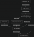
Stage 1: Power Generation & Storage
Components: Piezo, Rectifier (DB102S), Storage Capacitor (C1), Zener Diode (D1)
Stage 2: The Control Logic (Voltage Trigger)
Components: Voltage Comparator (TLV3011), Resistors (R1, R2)
Stage 3: The Microcontroller & Programming
Components: ATTiny10 (U2), 4-Pin Header (J1)
Stage 4: Output & User Interface
Components: MOSFET (Q1 - 2N7002), LED (LED1), Mode Switch (SW1)
I am very new with this (Usually using standard breadboard MCUs).
There was a question in my mind if I can build my own boards for a project at home.
Essentially I want to power a board with the electrical charge received from a Piezoelectric Sensor, and light up a few LEDs.
Basically this IC is designed to take the current from the Piezo and light up LEDS based on a 3p switch (Off/1 sec/3 sec) which will determine the state of the LEDs.
I did my research, and used GPT (Excuse my ignorance. LOL) but would always appreciate other people's opinions in this. Am I missing anything or is this over engineered?
I am a software guy, but I would really love to bridge the gap to this, and just trying to get a feel for IC designs and builds.
Items required:
| Ref Des | Quantity | Description | Key Specs / Notes | Estimated P/N Example |
|---|---|---|---|---|
| PIEZO1 | 1 | Piezoelectric Disc | 27mm-35mm diameter, brass plates, pre-wired | Murata 7BB-35-3 |
| BR1 | 1 | Miniature Bridge Rectifier | 100V, >100mA | Diodes Inc. DB102S |
| C1 | 1 | Electrolytic/Tantalum Capacitor | 220µF, 16V, Low-ESR | Panasonic ECE-A1EN221 |
| U1 | 1 | Voltage Reference/Comparator | Open-drain output, low power | TI TLV3011 |
| U2 | 1 | LED Flasher IC or Microcontroller | Programmed for 1/3/5 flash modes | Microchip ATTiny10-TSHR |
| Q1 | 1 | N-Channel MOSFET | SOT-23 package, logic level | ON Semi 2N7002 |
| LED1 | 5 | High-Brightness Green LED | 5mm, 1000+ mcd, 30° viewing angle | Lite-On L-7113GT |
| SW1 | 1 | Miniature Slide Switch | 3-position, through-hole | C&K JS202011AQN |
| R1, R2 | 2 | Resistors | 0805 or TH, values per circuit | 10kΩ, 100kΩ |
| D1 | 1 | Zener Diode | 5.1V, 500mW |
Connections:
Step-by-Step Schematic Connections
We will build the schematic in a logical order. Search for these parts in the EasyEDA library and place them on your canvas.
Stage 1: Power Generation & Storage
Components: Piezo, Rectifier (DB102S), Storage Capacitor (C1), Zener Diode (D1)
- Piezoelectric Disc:
- Place a Header-Male 1x02 (2-pin header). This represents where you will solder the wires from the piezo disc.
- Label the first pin PIEZO_IN.
- Label the second pin TARGET_GND. This pin will connect to the mounting magnets and the steel target.
- Bridge Rectifier (DB102S):
- The rectifier has 4 pins: two ~ (AC input), one +, one -.
- Connect the PIEZO_IN wire from the header to one of the ~ AC input pins.
- Connect the TARGET_GND wire to the other ~ AC input pin.
- The rectifier's - pin is now your circuit's main GND.
- The rectifier's + pin is the raw, rectified power. Connect this to:
- Storage Capacitor (C1 - 100µF-470µF Electrolytic):
- Connect the POSITIVE (+) leg of C1 to the rectifier's + pin.
- Connect the NEGATIVE (-) leg of C1 to the rectifier's - pin (GND).
- This capacitor is your main energy reservoir.
- Voltage Clamp/Regulator (Zener Diode D1 - 5.1V):
- Connect the Cathode (end with the band) to the + side of capacitor C1 (VCC).
- Connect the Anode to GND.
- This prevents the capacitor from charging above 5.1V and destroying the ATTiny10.
Stage 2: The Control Logic (Voltage Trigger)
Components: Voltage Comparator (TLV3011), Resistors (R1, R2)
- Voltage Comparator (U1 - TLV3011):
- This chip has 3 pins: V+, V-, OUT.
- V+ Pin (Power): Connect to VCC.
- V- Pin (Ground): Connect to GND.
- OUT Pin (Signal): This is our trigger signal. Connect it to:
- A 10kΩ Pull-up Resistor (R1): Connect between OUT and VCC.
- The INPUT of the MCU: Connect to Pin 2 (ADC1) of the ATTiny10.
- Voltage Reference (Resistors R2, R3):
- We need to set a threshold voltage for the comparator to trigger at (e.g., ~4.0V). We create this with a "resistor divider".
- Connect a 100kΩ Resistor (R2) from VCC to the comparator's IN+ pin.
- Connect a 33kΩ Resistor (R3) from the comparator's IN+ pin to GND.
- *(This creates about 4.1V at IN+, calculated as VCC * (R3/(R2+R3)) = 5V * (33k/133k) ≈ 4.1V)*.
- Connect the comparator's IN- pin directly to VCC. The comparator will output a LOW signal when VCC (IN-) falls below ~4.1V (IN+), which is perfect for detecting when a hit has charged the capacitor.
Stage 3: The Microcontroller & Programming
Components: ATTiny10 (U2), 4-Pin Header (J1)
- ATTiny10 (U2):
- Pin 5 (VCC): Connect to VCC.
- Pin 3 (GND): Connect to GND.
- Pin 2 (ADC1): Connect to the OUTPUT of the Voltage Comparator (U1). This is the trigger signal.
- Pin 1 (~RESET/~ADC0): This will be our mode select input. Connect it to one side of the Mode Switch (SW1).
- Pin 4 (OC0A): This is our output. Connect it to a 100Ω - 500Ω current-limiting resistor (R4), and then connect the other side of that resistor to the Gate of the MOSFET (Q1).
- Programming Header (J1 - Header-Male 1x04):
- This is only used to program the chip before soldering it to the board.
- Connect Pin 1 of the header to VCC.
- Connect Pin 2 of the header to the Gate of the MOSFET (Q1). This is the data line.
- Connect Pin 3 of the header to Pin 2 (ADC1) of the ATTiny. This is the clock line.
- Connect Pin 4 of the header to GND.
- Note: The exact programming pinout depends on your programmer. This is a common setup.
Stage 4: Output & User Interface
Components: MOSFET (Q1 - 2N7002), LED (LED1), Mode Switch (SW1)
- MOSFET (Q1 - 2N7002):
- Gate (G): Connect to the other side of current-limiting resistor R4 (from MCU Pin 4).
- Drain (D): Connect to the CATHODE (negative, short leg) of the LED.
- Source (S): Connect to GND.
- LED (LED1):
- CATHODE: Connected to MOSFET Drain (D).
- ANODE (positive, long leg): Connect to VCC through a small resistor (R5 - e.g., 10Ω). (Since our driver is on the ground side, this resistor protects the LED from inrush current).
- Mode Switch (SW1 - 3-Position Switch):
- The goal is to connect Pin 1 of the MCU to different voltages to represent different modes.
- Connect one outer pin of the switch to GND (Mode 1: 1 Flash).
- Connect the center pin (the wiper) to MCU Pin 1 (~RESET/~ADC0).
- Connect the other outer pin to VCC (Mode 3: 5 Flashes).
Attachments
-
 28.1 KB Views: 6