They are pretty much identical. If you are fine with n channels think about switching ground and Vcc for the P channel circuit and then replace the p channel with an N channel (keeping gate source and drain connections). Once you do a few times it will feel like second nature.
If you are switching a load then basically you don't calculate Vgs; you just switch the FET hard on. If the p-FET is specified as a "logic-level" type then Vgs = about -5V should do that. If it's not a logic-level type then Vgs = about -10V is the usual value.
If you are switching a load then basically you don't calculate Vgs; you just switch the FET hard on. If the p-FET is specified as a "logic-level" type then Vgs = about -5V should do that. If it's not a logic-level type then Vgs = about -10V is the usual value.
Vgs means "V(gate) minus V(source)". If the p-FET source is at 3.3V (Vcc) and the gate is at 0V then Vgs = V(gate) - V(source) = -3.3V.
To ensure the FET is switched fully on you would choose one with a rated Vgs(threshold) of around -1V.
Vgs means "V(gate) minus V(source)". If the p-FET source is at 3.3V (Vcc) and the gate is at 0V then Vgs = V(gate) - V(source) = -3.3V.
To ensure the FET is switched fully on you would choose one with a rated Vgs(threshold) of around -1V.
When the FET is turned fully on the voltage drop from drain to source will be small, determined by the product of current and the drain-to-source resistance Rds(on), which is a figure you'll find in the FET's datasheet. The lower the value of Rds(on) the better.
@Alec_t you said that vgs is simply the difference of the voltage at the gate and the source is this true for both p and n channel mosfet?
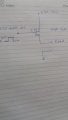
for my first example im going to use a p channel mosfet
assume that:
Vs= 15
Vg = 10
so my Vgs is simply = -5
and for my second example im going to use a n channel mosfet
assume that:
Vs= 0 (since source voltage is always at the ground level)
Vg = 10
so my Vgs is simply = 10
is this correct??? pls correct me if i have some error....TIA
That is definitely not true, there is no universal rule that says that an N-fet has to have its source connected to ground. Otherwise you have it correct.