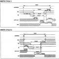
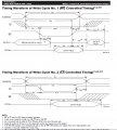
Hello all! I am new to this website and would like to get some assistance creating a functional circuit. Below are the lab directions:
Overview: Understanding memory
Resources to consult: Digital Electronics: Principles and Applications, 8th Edition, Chapter 11
Instructions:
1. Using the HM6116A120 (2Kx8 ram) create an addressable RAM circuit and perform the following:
2. Choose several address locations (not 0) and write the inverse of the address as data to that location.
a. Address is 0110 Data should be 1001
3. Read the memory in the following order: Read location 0 (this should be 0), Read the first location you wrote to, capture screen data, read the second location you wrote to, capture screen, etc.
4. Describe operation of the circuit. Capture output of seven segment for max, min, and in between values.
I am stuck on step 2a. I have tried a number of different avenues on how to wire it and none of them have been successful. I will show all four avenues I took to accomplish this. Additionally, I did research both the 6116 RAM chip and the 74LS244N buffer. Still at a total loss here.
Layout 1 (General Feedback into the Address Inputs):

Issues: Lights flicker; Read/Write function does not make a difference; No inversion takes place; No real memory takes place.
Operation: Only adjusted the Address Inputs and the WE position to enable Read or Write mode.
Layout 2 (Addition of a Pull-Up Resistors):

Remedies: Removes the flickering.
Issues: Read/Write function appears to be responsive; No inversion takes place; No real memory takes place.
Operation: Adjusted the Address Inputs, Data Outputs, and WE control.
Layout 3 (Removal of Pull-Up Resistors; Addition of Buffers; Addition of Pull-Down Resistor)

Remedies: None.
Issues: No functionality.
Operation: Adjusted Address Inputs, Control Inputs, and Data Outputs.
Layout 4 (Removal of Pull-Down Resistor; Movement of Buffers; Initiating New Outputs):

Remedies: None.
Issues: No functionality.
Operation: Still working this version of the circuit.
Any assistance, advice or even a complete revamp of the circuitry would be greatly appreciated. I'm highly methodical so step-by-step explanations work best for me. I have been at this lab now for about three days and now its mind numbing to look at. Maybe I'm over thinking this project.
Overview: Understanding memory
Resources to consult: Digital Electronics: Principles and Applications, 8th Edition, Chapter 11
Instructions:
1. Using the HM6116A120 (2Kx8 ram) create an addressable RAM circuit and perform the following:
2. Choose several address locations (not 0) and write the inverse of the address as data to that location.
a. Address is 0110 Data should be 1001
3. Read the memory in the following order: Read location 0 (this should be 0), Read the first location you wrote to, capture screen data, read the second location you wrote to, capture screen, etc.
4. Describe operation of the circuit. Capture output of seven segment for max, min, and in between values.
I am stuck on step 2a. I have tried a number of different avenues on how to wire it and none of them have been successful. I will show all four avenues I took to accomplish this. Additionally, I did research both the 6116 RAM chip and the 74LS244N buffer. Still at a total loss here.
Layout 1 (General Feedback into the Address Inputs):

Issues: Lights flicker; Read/Write function does not make a difference; No inversion takes place; No real memory takes place.
Operation: Only adjusted the Address Inputs and the WE position to enable Read or Write mode.
Layout 2 (Addition of a Pull-Up Resistors):

Remedies: Removes the flickering.
Issues: Read/Write function appears to be responsive; No inversion takes place; No real memory takes place.
Operation: Adjusted the Address Inputs, Data Outputs, and WE control.
Layout 3 (Removal of Pull-Up Resistors; Addition of Buffers; Addition of Pull-Down Resistor)

Remedies: None.
Issues: No functionality.
Operation: Adjusted Address Inputs, Control Inputs, and Data Outputs.
Layout 4 (Removal of Pull-Down Resistor; Movement of Buffers; Initiating New Outputs):

Remedies: None.
Issues: No functionality.
Operation: Still working this version of the circuit.
Any assistance, advice or even a complete revamp of the circuitry would be greatly appreciated. I'm highly methodical so step-by-step explanations work best for me. I have been at this lab now for about three days and now its mind numbing to look at. Maybe I'm over thinking this project.


