Anticipated Circuit Output?

Thread Starter

Glitchmobile

Joined May 8, 2010
10
Hi everyone, newbie here in many ways...

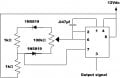
I've attached a circuit drawing that uses a 555 chip, and was hoping someone might
know what kind of output signal to expect at pin 3?
( I don't get a typical square wave, however don't know what kind of signal to expect).

The circuit output is to be connected to a mosfet's gate (not shown in drawing).
 

Attachments

ELECTRONERD

Joined May 26, 2009
1,147
In the AAC searchbar, type "555" and you get many results. In many of the numerous posts that pertain to the 555 timer, you'll also find a link to "Bill's Index" and several other links of his. I would recommend that you seek those links out within this forum.

Austin
 

Audioguru

Joined Dec 20, 2007
11,248
The output will be a rectangular wave with its duty-cycle adjusted by the pot making Pulse-Width-Modulation. PWM is used to control the brightness of a lamp or LED, the amount of heat from an electric heater and the speed of a DC motor.
 

Thread Starter

Glitchmobile

Joined May 8, 2010
10
Since pin 1 of the 555 timer is not connected to ground, the circuit won't work properly.
Thank you for the insight SgtWookie. I feel this is probably why my circuit was not operating correctly. When I put a scope to the circuit, all I got was a straight line, no square wave.
Thanks.
 

SgtWookie

Joined Jul 17, 2007
22,230
You are welcome.

I'm attaching a similar circuit, but it has needed parts that aren't in your schematic, some unnecessary parts have been removed, and the load on pin 7 has been decreased due to the value of R1 being increased to 1.5k.

There should always be a minimum of 100 Ohms per volt of Vcc between pin 7 and Vcc. If Vcc=12v, R1 should be at least 1.2k Ohms. If pin 7 has to sink more than 10mA, power dissipation in the timer will become excessive.

If you are going to drive a MOSFET gate with the PWM output, you will need to use a resistor between the 555 and the gate. I suggest using a resistor of between 10 and 62 Ohms, placed as close to the gate of the MOSFET as you can. If you omit the resistor, the "C" of the gate and the "L" of the wiring will cause the gate to "ring" when the charge level is suddenly changed. This will cause high power dissipation in the MOSFET.
 

Attachments

Thread Starter

Glitchmobile

Joined May 8, 2010
10
You are welcome.

I'm attaching a similar circuit, but it has needed parts that aren't in your schematic, some unnecessary parts have been removed, and the load on pin 7 has been decreased due to the value of R1 being increased to 1.5k.

There should always be a minimum of 100 Ohms per volt of Vcc between pin 7 and Vcc. If Vcc=12v, R1 should be at least 1.2k Ohms. If pin 7 has to sink more than 10mA, power dissipation in the timer will become excessive.

If you are going to drive a MOSFET gate with the PWM output, you will need to use a resistor between the 555 and the gate. I suggest using a resistor of between 10 and 62 Ohms, placed as close to the gate of the MOSFET as you can. If you omit the resistor, the "C" of the gate and the "L" of the wiring will cause the gate to "ring" when the charge level is suddenly changed. This will cause high power dissipation in the MOSFET.
Thanks for taking the time to elucidate the intricacies of the chip and accompanying parts, plus posting a similar circuit for further clarity. You're especially perceptive, in figuring that my objective is to control a MOSFET, spot-on.
 
Top