Amplifier to drive a Capacitor

Thread Starter

Mario Barbato

Joined Sep 10, 2015
8
Hello everyone,

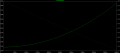
For my exam I have to design an amplifier to drive a 40nF capacitor. The signal is a trapezoidal wave that goes from 0 to 5V. Loop gain of my amplifier needs to be 8 from 0 to 200KHz. After a week I end up with the schematic in the picture.


However my output is not what i want even if my loop gain is almost 8. Moreover the system seems to be unstable, I tried to put a capacitor between base and collector of Q1, but doing this the output is broke down.


1) How can I reduce the delay in the output?
2) How can I make the amplifier stable?

Sorry for my english and thank you all for the answers.
 

Attachments

Tako

Joined Oct 21, 2014
65
You have very low value of resistors R6 and R7 in the loop. For Vout = 35 V, the current through R6 and R7 is:

Vout / (R6 + R7) = 35 / 10 = 3.5 A

Is it intended?


Is your project discrete or integrated?


Two another remarks:
1) I don't get how it is possible that you get positive Vout while having positive Vin.
Vin up -> V+ down -> 2nd stage up -> Vout down

2) Your inverter. There is something wrong. The drain of NMOS is connected with the body. The same for PMOS.


Do you have any requirements for your project? I do not get why you started with such a design, that is, emitter resistors in the 1st stage, specific current mirror in the 1stage, 2nd stage fixed gain. Why didn't you started with the simplest architecture like Fig. 3.2 here: https://payhip.com/b/5Srt (click Preview button) to see whether your specs are met and then to add buffer (common drain architecture) as a 3rd stage or use another architecture?
 

Thread Starter

Mario Barbato

Joined Sep 10, 2015
8
You have very low value of resistors R6 and R7 in the loop. For Vout = 35 V, the current through R6 and R7 is:

Vout / (R6 + R7) = 35 / 10 = 3.5 A

Is it intended?


Is your project discrete or integrated?


Two another remarks:
1) I don't get how it is possible that you get positive Vout while having positive Vin.
Vin up -> V+ down -> 2nd stage up -> Vout down

2) Your inverter. There is something wrong. The drain of NMOS is connected with the body. The same for PMOS.


Do you have any requirements for your project? I do not get why you started with such a design, that is, emitter resistors in the 1st stage, specific current mirror in the 1stage, 2nd stage fixed gain. Why didn't you started with the simplest architecture like Fig. 3.2 here: https://payhip.com/b/5Srt (click Preview button) to see whether your specs are met and then to add buffer (common drain architecture) as a 3rd stage or use another architecture?

The architecture was an advice of the professor, but I will look at the link to get more knowledge about the topic.
The current on the feedback resistors is not intended, I just computed them to impose the closed loop gain = 8.

System is discrete and its specifications are:
0 to 40V output
Max Distorsion=0.1%
Slew rate=100V/us
Max supply voltage= 55V

1) I need a positive output so i used a pnp differential pair to obatin Vin up -> V+ down, then invert it using the CE stage.
2) Isn't it the push-pull architecture?
 

Thread Starter

Mario Barbato

Joined Sep 10, 2015
8
What is V+ at the base of Q1?
Why are all your resistor values so low?
V+ is the positive output of the differential pair.
I'm not so practical of resistor values, I calculated them considering Ic=100mA, Vbe=0.7V, Vce=10V for all the transistors and Vcc=50V
 

Tako

Joined Oct 21, 2014
65
Ok, my mistake:

M2 - PMOS
M1 - NMOS

3rd stage is a buffer.

Try to change values of resistors in the feedback loop by the factor of 1.000. So you have:

R7 = 8.75 kOhms
R6 = 1.25 kOhms

We will see if you hit current driving capabilities when using so low resistors.
 

Thread Starter

Mario Barbato

Joined Sep 10, 2015
8
Ok, my mistake:

M2 - PMOS
M1 - NMOS

3rd stage is a buffer.

Try to change values of resistors in the feedback loop by the factor of 1.000. So you have:

R7 = 8.75 kOhms
R6 = 1.25 kOhms

We will see if you hit current driving capabilities when using so low resistors.
With these values the system is still unstable, there isn't a really change in the behaviour even if the output wave seems to be better.
I'm trying to redisgn everything, but the differential pair is triggering me :)
 

Bordodynov

Joined May 20, 2015
3,180
Bad scheme. A complex current mirror operates in a very poor mode, just like a differential cascade. Leave a simple current mirror. Next, remove (short-circuit) the resistor in the emitter of the transistor of the second cascade. Add emitter followers to the differential cascade circuit. Give an offset for the output stage so that through the MOS transistors the current flows at least 10-15 mA. Resistors in the feedback increase in 1000 times. If you get a small stability (ringing), then add a series of chains from the capacitor and the resistor between the collectors of the differential cascade.
 

Tako

Joined Oct 21, 2014
65
I think resistors should be increased, also suggested by Bordodynov. Stability is another thing that should be taken care of. Step by step and you will have everything. For the stability, Miller capacitor should be used then zero-nulling resistor added to tune the phase margin. The compensation should be done in the 2nd stage - base-collector on npn.
 

Thread Starter

Mario Barbato

Joined Sep 10, 2015
8
Bad scheme. A complex current mirror operates in a very poor mode, just like a differential cascade. Leave a simple current mirror. Next, remove (short-circuit) the resistor in the emitter of the transistor of the second cascade. Add emitter followers to the differential cascade circuit. Give an offset for the output stage so that through the MOS transistors the current flows at least 10-15 mA. Resistors in the feedback increase in 1000 times. If you get a small stability (ringing), then add a series of chains from the capacitor and the resistor between the collectors of the differential cascade.
How do I introduce an offset? Using an AB push-pull or simply using two resistor connected to de drain of M1 and M2?
 

Bordodynov

Joined May 20, 2015
3,180
I advise you to see how the input stage of the operational amplifier LM324 is arranged. Look at the circuitry of the output stages of audio amplifiers operating in the AB class. Especially those that are built on MOS transistors. A simple correction using a single Miller's capacitance will not help (this is my opinion). This is due to the large additional phase shift due to the capacitive load.
 

Thread Starter

Mario Barbato

Joined Sep 10, 2015
8
I advise you to see how the input stage of the operational amplifier LM324 is arranged. Look at the circuitry of the output stages of audio amplifiers operating in the AB class. Especially those that are built on MOS transistors. A simple correction using a single Miller's capacitance will not help (this is my opinion). This is due to the large additional phase shift due to the capacitive load.
Ok thanks a lot for your advice! :D
 

Tako

Joined Oct 21, 2014
65
If the output capacitance dominates, the compensation will be achieved using the output capacitance. The same is done in a regulator application.

The point is to work on the schematic step by step. One change then simulation. Another change and simulation. And so on. Approaching a lot of problems at once usually does not give expected results and does not teach a lot.

If bigger resistors in the feedback loop helped for the shape of the output voltage you should leave new values. AC characteristic is done in the open loop simulation, so their values would rather not help for that. If the output dominates, you would like to increase its value as suggested at the beginning of this post. Lead compensation may also be used to tune the phase margin.
 
Top