Facebook
 Google
 GitHub
 Linkedin
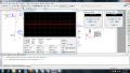
Yes indeed I meant I used a 2N3904. Thank you, perhaps you would like a new career picking up my typos? I can promise you plenty of work.Your circuit is alm,ost saturated. Every transistor is different so some will be saturated and some will not be saturated.
Why not design the circuit properly so it works with all 2N3904 transistors?
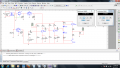
The circuit uses a 2N3904 NPN transistor but you tested it with a 2N3906 PNP transistor which is completely different.
A single transistor can easily provide a voltage gain of only 100. Bypass the emitter resistor with a capacitor.

And yes I suggested, way back in this thread to revise the biasing to the middle as normal and reduce the drive, but this bit of the design is not mine it is yours and the OP's.