Facebook
 Google
 GitHub
 Linkedin
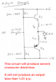
You haven't satisfied all the requirements of your project with your circuit since both your compound transistor (Q1_Q4) and Q2 use voltage divider biasing and you have to have two types.
What happened to Q3?
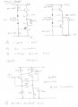
Here are some suggestions based on what we have been saying. There are both single and split supply versions. Try these in MSim. Make sure you gets the capacitors the right way round, although I don't think MSim distinguishes.
If you like them we can move on to the limiter.
What happened to Q3?
Here are some suggestions based on what we have been saying. There are both single and split supply versions. Try these in MSim. Make sure you gets the capacitors the right way round, although I don't think MSim distinguishes.
If you like them we can move on to the limiter.
Attachments
-
 46.9 KB Views: 16
")