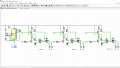
It would greatly help clarify the schematic if you just used the ground symbol at each component ground, instead of running ground lines all over the schematic.
Also do the same for Vcc.
As is, the schematic is way too busy.
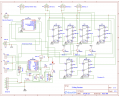
It would greatly help clarify the schematic if you just used the ground symbol at each component ground, instead of running ground lines all over the schematic.
Also do the same for Vcc.
As is, the schematic is way too busy.
Referring to the circuit in post #55 - Still two relays per device, so while the logic structure is different, I don't see any clear advantage over the other solutions.
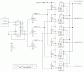
I needed inverters so used 40106B. I could have used 4093's, not use U11, and then used the remaining one for a clock generator instead. The CHARGn and OPERn resistors are used for sim purposes only. The logic works in simulation per the TS chart posted at the beginning of this thread.
It would greatly help clarify the schematic if you just used the ground symbol at each component ground, instead of running ground lines all over the schematic.
Also do the same for Vcc.
As is, the schematic is way too busy.
Here is the first pass at the circuit I described in posts #12 and 37, with some updates. There are no logic steering diodes because they are not needed. There is no deadband circuit at the node labeled Relay Power because the TS thinks it might not be needed.
Operate, Charge, and the three devices must share a common GND (not shown). There is complete galvanic isolation between the devices and the controller, so the devices do not have to share a common ground with the controller. They could be AC induction motors, RF signals, etc, as long as the relays are designed for them.
Also, relay power can be greater or less than logic power as long as they share a common GND. For example, this could be a 5 V circuit with 24 V relay coils. If the coil current is greater than 100 mA, the three transistors and the suppression diodes will have to be beefed up.
Definitely.
I didn't check every wire, but it would appear to be basically okay.
Does the sequence need to start in any particular order when power is applied?
If so, you will need to add a power-on reset to U1.
Also make sure are CMOS device input (not outputs) are connected high or low.
Some appear unconnected on your schematic
Never leave a CMOS input open or you may get flaky results.
Okay, that circuit works without added logic because there is no deadband circuit.
"Might not be needed" is not sufficient reason for me to not do it.
I think using DPDT relays instead of SPDT relays is worth it to insure there is no crossover conduction when the states are changed.
Hmm, there seems to be a difference in interpretation among us. I was under the impression that there were 3 completely separate devices, each with its own battery charger and load. Others seem to think they’re one load and one charger with 3 batteries.
So, to the TS: which is it?
Edited to add: AKs circuit seems to use the second interpretation, since it has only one wire for charger and load, and 3 for the devices, whatever that means.
I haven’t figured all that out yet but, to give an example off the top of my head with using a battery: in the ‘operating’ mode the battery will be powering a 10W light; in the ‘charging’ mode it will be receiving about 14V DC from a mains charger, and in ‘shut off’ mode it will be doing nothing. Is that what you mean?
The reason why I’m not going down the microprocessor route is so I can also show it to one of my students and clearly point out the different functions being carried out by each section of the circuit. You can’t do that pointing to a monolithic processor chip.
So....there are 3 batteries, 1 charger and 1,10W load for the whole system. And the three batteries are rotated between the charger, the load, and disconnected?
In my read of the system, Charge and Operate are two separate power sources with a common GND, that are common to the three devices. The three devices are the destinations for the power.
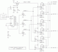
Here is an updated version of the 6 x SPST circuit that includes cross-conduction prevention.
R1 holds Q4 on most of the time. A positive clock edge is coupled through C2, raising the gate voltage high enough to turn off Q4. Because the Q4 gate voltage necessary to drive two relay coils is less than 7.6 V, the differentiated pulse period will be less than one time constant. To account for this, C2 is 1.0 uF for an intended 50 ms pulse period.
Since pairs of relay coils are in direct parallel, three suppression diodes are removed.
Note that Q4 and the relays are not recommended part numbers; they are what is in my design libraries.
UPDATE: Now that the TS has explained why brief periods of cross-cionduction are not a problem, Q4 and its parts are not needed. This takes us back to the schematic in #105.
Okay, so that basically does everything my circuit does.
So now the tradeoff is between using DPDT relays, versus SPDT relays with the added MOSFET circuit that prevents overlap.
There seems to be confusion over the configuration of the whole system. There are 3 devices, let them be batteries since they can deliver power and receive power in charging, and each of those 3 batteries can be in one of three states; delivering power, being recharged or idle.
This is what my initial ‘truth table’ showed and also that no battery (device) can be in the same state as the other two so there is no overlap, although in practice a little would not be a problem.
There is only one load for the three batteries to deliver to in turn and equally one charging system. So it’s not a load and charger for each device.
I’m hoping that the schematic I have produced, based on Crutschow’s relay design, will do the job but the only way I will know is to build it. Getting the PCB designed and printed will take about 2 weeks and then assembly and testing another couple of weeks so my thinking is that by early November I will know how well it works.
The other designs suggested may also work equally well, and thank you everyone for all the input, but I had to choose one and this one shows the train of events in a more open and electromechanical way as a teaching tool. It’s reminiscent of the approach used in a manufacturing context as per ‘ladder logic’.
More modern approaches used microprocessors and such but they would be harder to diagnose by following the causal chain through the process. There’s also less to see from the outside.
It is interesting how going from switching two devices to three results in such a big jump in complexity - I’m sure there are lots of fascinating spinoffs re the mathematics of permutations.
So now it’s on to ‘proof of pudding’ stage . . . .
Definitely.
I didn't check every wire, but it would appear to be basically okay.
Does the sequence need to start in any particular order when power is applied?
If so, you will need to add a power-on reset to U1.
Also make sure are CMOS device input (not outputs) are connected high or low.
Some appear unconnected on your schematic
Never leave a CMOS input open or you may get flaky results.
Yes, this is a point I made earlier, that I need to be able to move the switching round to a particular state e.g. device 2 charging, and so how could I advance the sequence manually.
My initial suggestion is by having the two timer intervals, with one of them being short so it would quickly move round to the desired state, and then the other timer interval is selected to start the ‘run’.
However, from what you say, putting a high on to pin15 of U1, with a ‘push button’ for example, might do this? But won’t that just reset the relays back to state 1 (4017 Q0 output high) rather than move it forward one at a time till the desired state is reached?
Which CMOS inputs have I left floating? I’m still recovering from ‘snow blindness’
It would help tremendously if instead of presenting a "Hypothetical" problem,
a "real-World" problem was presented.
It seems to me that, not only is this a poor solution,
( "one Battery idle" when it could be being Charged ), ( there is no practical reason for an "idle-Battery" ),
but that the external "visual" qualities do not contribute any value
towards the actual understanding of how, or why, the Circuit operates,
especially when constructed on a Printed-Circuit-Board, and with Relays sealed in little blue plastic boxes.
Take your Students on a field-trip to a local High-Rise-Building and show them the operation
of a huge Delta-Wye Motor-Starter for a ~200 horsepower Water-Chiller-Plant.
And, get a copy of the Schematic for them to analyse before, and after, the visit.
.
.
.
It would help tremendously if instead of presenting a "Hypothetical" problem,
a "real-World" problem was presented.
It seems to me that, not only is this a poor solution,
( "one Battery idle" when it could be being Charged ), ( there is no practical reason for an "idle-Battery" ),
but that the external "visual" qualities do not contribute any value
towards the actual understanding of how, or why, the Circuit operates,
especially when constructed on a Printed-Circuit-Board, and with Relays sealed in little blue plastic boxes.
Take your Students on a field-trip to a local High-Rise-Building and show them the operation
of a huge Delta-Wye Motor-Starter for a ~200 horsepower Water-Chiller-Plant.
And, get a copy of the Schematic for them to analyse before, and after, the visit.
.
That's because of arbitrary-rules,
not because there aren't a ton of very experienced engineers here who only
took-up the challenge to relieve their boredom.
Try asking something like,
"how would You demonstrate, and create interest in, an easy to build project
that has a valuable purpose, and is easy to visually understand" ?
My initial suggestion is by having the two timer intervals, with one of them being short so it would quickly move round to the desired state, and then the other timer interval is selected to start the ‘run’.
However, from what you say, putting a high on to pin15 of U1, with a ‘push button’ for example, might do this? But won’t that just reset the relays back to state 1 (4017 Q0 output high) rather than move it forward one at a time till the desired state is reached?
Correct. Pin 15 is the Reset input. Forcing it high at any time will in fact force the circuit into state 1. There is a possibility that the 4017 could power up in state 5, for example, and it would take five clock pulses before the circuit was back to state 0. To prevent this, a POR (Power On Reset) circuit can be added with 2 resistors, 1 diode, and 1 capacitor. This would be an automatic function, no buttons involved.
Separate from that is a manual advance. One way to do this is to force the Clock input (pin 14) high when it is in the low state. It is a bit more complex that with the Reset input because of switch bounce. When switch contacts come together, they don't just come together. They almost always bounce together-apart-together-apart for a few milliseconds. You may press the button once, but the circuit sees 15 transitions. Of course there is a way to mitigate this. But wait, there's more. If you press the Advance button while the Clock signal already is high, nothing will happen. If the output of the Clock Source circuit is a 50/50 square wave, the high part of the signal could be 30 seconds long. Of course, there is a way to mitigate this, also.
Having two clock periods ("timer intervals") probably is the more simple solution, but the circuit in #104 has a possible issue. During the operation of SW2, there is point when neither pot is connected. As long as the oscillator does not jump up to a megahertz frequency, this is not a huge problem because whatever this does to the clock timing is divided by at least 4096. But a better way to go is to have the normal-mode pot connected permanently to R15, and the set-mode pot switched in parallel with it. Now, the switch requirement is SPST, not SPDT, and it can be any simple, bouncy pushbutton switch.

 Facebook
 Google
 GitHub
 Linkedin