9600 bps transistor switch issue

Thread Starter

hemuz

Joined Mar 7, 2010
14
hi all

i am making a receiver circuit that`s receive signal from computer serial port in optical form , the receiver takes the signal by a photo-transistor and gives the logic 1 (3.3v) and 0(0v) to micro controller.

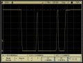
the circuit i built works properly in 2400 bps, but their`s a delay in logic(1) rising in case of 9600 bps, can any one help me to find the reason , noting that the transistors i use support high speed switching much more 9600bps.

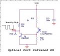
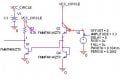
attached the signal i get in 9600bps and 2400bps and the circuit i make.

thanks
 

Attachments

hgmjr

Joined Jan 28, 2005
9,027
Reduce R18 to say 4.7K.

The risetime of the voltage at the collector is influenced by the value of the collector load resistor and the transistors internal collector capacitance. Reducing R18 will reduce the risetime at the transistor's collector.

hgmjr
 

Thread Starter

hemuz

Joined Mar 7, 2010
14
Reduce R18 to say 4.7K.

The risetime of the voltage at the collector is influenced by the value of the collector load resistor and the transistors internal collector capacitance. Reducing R18 will reduce the risetime at the transistor's collector.

hgmjr
hi hgmjr

thank you for your relpy ,but the problem in the 1st stage , the time delay appears at the base of the transistor , the delay in falling on the transistor base in the reason of the delay of the rising signal in the collector , can you suggest solution for this

thanks again for replying
 

hgmjr

Joined Jan 28, 2005
9,027
If you scroll down in the AAC article to which I have link in the above post, you will see a figure containing two current mirror circuits (a) and (b). I would direct your attention to the one using two NPN transistors. If you replace the resistor labeled Rbias with your phototransistor and then take your output from the collector of the transistor with Rload in its collector circuit, you should be able to get an improved performance from your phototransistor.

hgmjr
 

Thread Starter

hemuz

Joined Mar 7, 2010
14
If you scroll down in the AAC article to which I have link in the above post, you will see a figure containing two current mirror circuits (a) and (b). I would direct your attention to the one using two NPN transistors. If you replace the resistor labeled Rbias with your phototransistor and then take your output from the collector of the transistor with Rload in its collector circuit, you should be able to get an improved performance from your phototransistor.

hgmjr
dear hgmjr

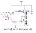
Thank you again , i think that this solution will make a path for high current flow through the photo-transistor and the the transistor that`s connected to make a diode as shown in the attached picture that`s will lead to make a drop in the low current capacitor power supply i use , can we put a resistor somewhere that can serve the speed of switching of data and limits the current ?

hemuz
 

Attachments

hgmjr

Joined Jan 28, 2005
9,027
dear hgmjr

Thank you again , i think that this solution will make a path for high current flow through the photo-transistor and the the transistor that`s connected to make a diode as shown in the attached picture that`s will lead to make a drop in the low current capacitor power supply i use , can we put a resistor somewhere that can serve the speed of switching of data and limits the current ?

hemuz
Actually there is never going to be any significant current flowing in the phototransistor unless it fails. I don't think you are going to have to worry about power dissipation.

What is the highest frequency you can now respond to with this arrangement?

If you are familiar with the plots for the collector current versus Vce, then you will notice that the current mirror does not allow the phototransistor to saturate. That tends to make the phototransistor exhibit its fastest response time. That is because the load line is pretty much a vertical line unlike the case where you permitted the phototransistor to saturate.

hgmjr
 

Thread Starter

hemuz

Joined Mar 7, 2010
14
Actually there is never going to be any significant current flowing in the phototransistor unless it fails. I don't think you are going to have to worry about power dissipation.

What is the highest frequency you can now respond to with this arrangement?

If you are familiar with the plots for the collector current versus Vce, then you will notice that the current mirror does not allow the phototransistor to saturate. That tends to make the phototransistor exhibit its fastest response time. That is because the load line is pretty much a vertical line unlike the case where you permitted the phototransistor to saturate.

hgmjr

Dear hgmjr

i`ll try this experimentally and give you the result of the maximum data rate that`s this configuration supports , Mr.hgmjr Thanks very much for your help and support.

BEST REGARDS
Hemuz
 

hgmjr

Joined Jan 28, 2005
9,027
I look forward to feedback from your testing.

Keep in mind that now that you have this arrangement, you will be at liberty to adjust the value of the collector load resistor in the output transistor to the most optimum value since it is isolated from the phototransistor by the current mirror circuit.

hgmjr
 

Thread Starter

hemuz

Joined Mar 7, 2010
14
back again ,

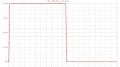
i tried to simulate the circuit in the orcad using a normal transistor instead of photo-transistor , by measuring the response it`s OK , but when i measured the current flowing in case if the photo-transistor on , it was very massive it`s about 8A , dear hjmgr can you show me how this circuit works without high power dissipation in case of the photo-transistor conducts and seems like very low resistance?

attached the circuit and result of simulation

thanks

hemuz
 

Attachments

hgmjr

Joined Jan 28, 2005
9,027
back again ,

i tried to simulate the circuit in the orcad using a normal transistor instead of photo-transistor , by measuring the response it`s OK , but when i measured the current flowing in case if the photo-transistor on , it was very massive it`s about 8A , dear hjmgr can you show me how this circuit works without high power dissipation in case of the photo-transistor conducts and seems like very low resistance?

attached the circuit and result of simulation

thanks

hemuz
What you must keep in mind is that a phototransistor cannot achieve the same saturation currents that can be achieved with an ordinary transistor. It is not accurate to model a phototransistor with a standard transistor.

Do you have the part number for the phototransistor that you plan to use in your circuit? Then I can gauge better the maximum power you are likely to encounter.

hgmjr
 

Thread Starter

hemuz

Joined Mar 7, 2010
14
What you must keep in mind is that a phototransistor cannot achieve the same saturation currents that can be achieved with an ordinary transistor. It is not accurate to model a phototransistor with a standard transistor.

Do you have the part number for the phototransistor that you plan to use in your circuit? Then I can gauge better the maximum power you are likely to encounter.

hgmjr
this is the datasheet of the photo-transistor


in the data sheet page 6

Precautions For Use
1. Over-current-proof
Customer must apply resistors for protection , otherwise slight voltage shift will cause big
current change ( Burn out will happen ).

hemuz
 

Attachments

hgmjr

Joined Jan 28, 2005
9,027
That's helpful.

Take a look at the plot of Vce against Ic. You will notice that the maximum current it represents is 10 milliamps. Even if it goes to the device maximum of 20 milliamps, the power dissipation will only reach 2.6V times 20 milliamps which only reach 52 milliwatts.

hgmjr
 

Thread Starter

hemuz

Joined Mar 7, 2010
14
That's helpful.

Take a look at the plot of Vce against Ic. You will notice that the maximum current it represents is 10 milliamps. Even if it goes to the device maximum of 20 milliamps, the power dissipation will only reach 2.6V times 20 milliamps which only reach 52 milliwatts.

hgmjr

nice !!!! , understood, this is so good , :) the next step is building the circuit and test it . i`ll put the result in this topic , Really Mr.hgmjr this is wonderful help from you ,

Thaaaaaaaaanks

Hemuz
 

Thread Starter

hemuz

Joined Mar 7, 2010
14
Great , the circuit works properly to data rate near 28000 bps ,

Great thank you for hgmjr for help in this issue solving .

Best Regards

Hemuz
 

hgmjr

Joined Jan 28, 2005
9,027
Great , the circuit works properly to data rate near 28000 bps ,

Great thank you for hgmjr for help in this issue solving .

Best Regards

Hemuz
That is excellent news. Glad you were able to achieve performance in excess of that which you were seeking.

hgmjr
 
Top