555-PWM Motor Control - MOSFET gets hot

sghioto

Joined Dec 31, 2017
8,762
I tried using the IRF540 for low side switching but it remained fully on at all times, so need to dig further into that (assuming with source being GND and not a capacitance this changes things.
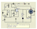
The 555 driver in post #1 is unconventional. Try this circuit.
With the values shown the PWM varies from 5 to 95% while the frequency remains fairly stable at appx 550hz.
Changing Rv1 to 10K and C1 to 220nf varies the PMW from 10 to 90% at appx 450hz
1794598574038.png
 
Last edited:

kiroma

Joined Apr 30, 2014
325
Ringing is usually an issue on the drain side (load L with drain C) when fet turns off. Adding a proper snubber will rid ringing. I had this design issue when driving fuel injectors.

It can also happen on the gate side. The scope is the only way to see what's going on there.
Yeah, I was talking about the gate side, thought you were talking about the same thing.
I agree with you.
 

DC_Kid

Joined Feb 25, 2008
1,251
The 555 is likely just the wrong approach, way too many discrete parts, and the 555 is not really a clean PWM.
I did a PWM driver using a 5v trinket coded with ckt-python. 12v is the power, 5v regulator is needed, and still needs a pre-driver fet or opto between trinket and the IRFZ. I have two pots, one changes PWM from 1-50% (because it's an up pulse, so beyond 50% is not needed), and the other pot does freq from 1-100. These ranges can be changed via code. I built my MC for my TIG welder to get pulse ability on a machine that did not have that feature.

So although the 555 ckt presented is a good learning schematic, I would look elsewhere to make something solid and easily changed (coded). These days, MC's like Trinket and ESP32 are ez to deal with. Heck, an ESP32 can run ssh and wifi, so can get a shell over wifi, edit a .py, and restart it.

I like ez.
 

MisterBill2

Joined Jan 23, 2018
28,550
At the very least, for actual PWM conrol, there is a requirement to actually switch that IRFZ540 OFF. That appears to be lacking in the circuit in post#21.The gate control will not pull down that far, I dont think.
 
Last edited:

DC_Kid

Joined Feb 25, 2008
1,251
I would at least park a 200-400ohm pull-down on the gate.
The 555 has limted source current. The 555 itself should also pull down pretty close to gnd.
 

MrAl

Joined Jun 17, 2014
13,887
Hello again,

Ringing comes from the combination of values of R, L, and C in a simple RLC circuit. The values tell us if the circuit is overdamped, underdamped, or critically damped by way of the discriminant. The discriminant is probably called that because it allows us to discriminate between those three cases.
For example, the discriminant for a series RLC circuit driven by a voltage source is:
D=C*R^2-4*L
and as we see there are four values R, L, and C.
Now if D is positive, the circuit is overdamped so there is no ringing, and
if D is negative, the circuit is underdamped and there could be very little ringing or a lot of ringing, and
if D is zero, the circuit is critically damped so there will be no ringing.

In MOSFET drive circuits the most important part is the source circuit because that causes feedback to the gate which is caused by unwanted modulation of the source terminal. That is very important because it can cause the MOSFET to turn on and off repeatedly while it tries to transition between some 'on' state and some 'off' state. The total inductance is the culprit there because series inductance in the source circuit makes the source terminal look like it is not properly grounded.
This is similar to how negative resistance works in an NPN common emitter circuit with an emitter resistor, except it is much more dynamic.
Imagine if you applied a gate signal of +10v to the N MOSFET and the source terminal suddenly rose up to +9v. That would mean instead of the gate to source seeing +10v, it would only see +1v. What actually happens though is it first sees +10v, turns on, and then the source terminal voltage rises to +9v and then the MOSFET turns off again, which causes the source terminal voltage to drop to 0v again, which in turn means the gate to source now sees +10v again which makes the MOSFET turn on again, and this happens over and over again. That's the modulation of the source terminal that really messes up the whole switching transition and causes a lot more power dissipation.
So we not only have the R, L, and C to think about, we have to think about the L in the source circuit with even more attention.
 

DC_Kid

Joined Feb 25, 2008
1,251
Using the general LRC to define ringing on the gate side is not that simple.
But even if using general LRC math the L needed to get a ring from a gate that has near 3.33nF @ 12v (~30nC), the L would be magnitudes smaller than a 4" piece of 22awg wire connecting gate to the 555.

(using some guessing on wiring)
3.33nF with wire of near 100nH w/ approx 26mOhm in wiring, the ringing would be near 8.72MHz, but would last only 3x114ns, and it tapers off very fast (just 3 periods), likely just the initial 1st and 2nd peak at a voltage high enough to have fet on, but it's happening very fast, faster than what that fet spec sheet says the max on/off freq could be. I would say a ringing that is below 5MHz could be practical consideration, but even with that I don't think it would cause fet to heat up.

My hypothesis, its not an LRC ringing issue on the gate.

I might suspect the 555 output is not reaching 10v as the frequency is turned up?
 
Last edited:

MrAl

Joined Jun 17, 2014
13,887
Using the general LRC to define ringing on the gate side is not that simple.
But even if using general LRC math the L needed to get a ring from a gate that has near 3.33nF @ 12v (~30nC), the L would be magnitudes smaller than a 4" piece of 22awg wire connecting gate to the 555.

(using some guessing on wiring)
3.33nF with wire of near 100nH w/ approx 26mOhm in wiring, the ringing would be near 8.72MHz, but would last only 3x114ns, and it tapers off very fast (just 3 periods), likely just the initial 1st and 2nd peak at a voltage high enough to have fet on, but it's happening very fast, faster than what that fet spec sheet says the max on/off freq could be. I would say a ringing that is below 5MHz could be practical consideration, but even with that I don't think it would cause fet to heat up.

My hypothesis, its not an LRC ringing issue on the gate.

I might suspect the 555 output is not reaching 10v as the frequency is turned up?
Hi,

I thought I made it clear that the source terminal is responsible for a lot of the ringing because of the series inductance. The sequence is like this...

The gate voltage rises, the mosfet turns on, the source inductance does not allow current to flow immediately so the source terminal voltage rises, which reduces the turn-on gate voltage, which turns the mosfet off. The mosfet turning off means the source terminal voltage again becomes lower, so the mosfet turns back on, the inductance now has a small current due to the inductor current ratcheting so the source terminal does not rise as much as it did originally, so the gate voltage does not fall as much as it did before, so the mosfet stays on a little harder, but still not enough, which means the mosfet turns off again. The source terminal voltage again drops, the gate voltage rises again, the mosfet turns back on. The inductor current by now has ratcheted up higher so the source terminal stays lower so the gate voltage stays higher which keeps the mosfet on a little more than before.
After a number of these pseudo on/off cycles, the mosfet gate to source voltage eventually stabilizes and the mosfet stays on. I am calling then "pseudo" on/off cycles because the mosfet does not always turn perfectly off or completely on, the drain to source could be partly conductive where the conductance rises with each cycle.

That's the theory behind the gate to source voltage and the source voltage itself, and the drain voltage ends up being modulated along with the DS current. That is why we have to pay a lot of attention to the source circuit and the way the driver feeds the gate and source terminals.

Now resonant switching is a lot more complicated but then that is an entirely different subject area really than purely pulsed operation.
 

DC_Kid

Joined Feb 25, 2008
1,251
@MrAI,
It's why I mentioned having a scope on the gate is the only way to see what's going on. Placing probe directly onto FET package terminals.

Although the Vgs is affected in the ways you described, I highly doubt that is the issue here.

There's also another place to look. Is the ext diode on motor the correct type/size? If it fails to do it's job, there will be avalanche scenario, which can cause the FET to heat. With big L motors I would place a 50v TVS or fat zener between DS of the FET.

There's also simple FET reverse biased via the body diode, and with a Vdrop of ~1.5 any reverse current could also heat the FET. This would be very unusual to see using the schematic as seen in this thread.

These issues really need a scope. ;)
 
Last edited:

MrAl

Joined Jun 17, 2014
13,887
Ringing is a relation of R, L, and C. So, too low resistance will increase the ringing, and higher inductance will also increase it. Higher C, on the other hand, will decrease it.
Hi,

But this is a specific application: driving a MOSFET (such as an N channel device). It's not a simple RLC circuit, for one there is feedback between source and gate, and also drain and gate. The values of L and C can actually switch roles in a circuit with feedback, and a delay can cause ringing.

But then there is the application itself. For example, which 'C' would you increase to lower the ringing in the common source MOSFET N channel switching circuit.
 

MrAl

Joined Jun 17, 2014
13,887
@MrAI,
It's why I mentioned having a scope on the gate is the only way to see what's going on. Placing probe directly onto FET package terminals.

Although the Vgs is affected in the ways you described, I highly doubt that is the issue here.

There's also another place to look. Is the ext diode on motor the correct type/size? If it fails to do it's job, there will be avalanche scenario, which can cause the FET to heat. With big L motors I would place a 50v TVS or fat zener between DS of the FET.

There's also simple FET reverse biased via the body diode, and with a Vdrop of ~1.5 any reverse current could also heat the FET. This would be very unusual to see using the schematic as seen in this thread.

These issues really need a scope. ;)
Hi,

Oh a scope is a good idea for sure, just have to be a little careful with the gate terminal.

Not sure what you mean about the Vgs. What kind of MOSFET are you using and how is it connected now?

There is also the gate rise and fall times. By shaping the ramp up and ramp down any oscillations can be dampened. We used that I deal in circuit that had to drive high current MOSFETs a long time ago. Series gate resistance can help control this.

The other thing funny about capacitance is that increasing it can cause a higher PEAK to form, even though it may in some cases decease the actual settling time.
 
Last edited:

DC_Kid

Joined Feb 25, 2008
1,251
555 has push pull output (BJT variant that is mentioned here).
What does the output do when the 555 loses power (stops working) for some unforeseen reason, or it's sink transistor fails in some odd way? A pull down helps to protect the power end (fet / load).

If the 555 push sticks on, the motor goes full speed. This scenario should also be mitigated if a full speed non-controlled motor is a bad event, etc.

There's "it works", and then there's "well designed". As of now, probably just a linear region issue as the freq goes up on the 555.
 

MrAl

Joined Jun 17, 2014
13,887
555 has push pull output (BJT variant that is mentioned here).
Hi,

This is interesting because the BJT version I think has a totem pole output and that (i also think) goes to a high impedance state when no power to the 555.
This can look like an unusual input to a MOSFET, and may cause either an indeterminant state, or pseudo memory of the last state. If there is something else with the MOSFET it could feed back through the 555 output and actual partially power up the 555 at its supply rail which can result in very unusual behavior. This might happen if there was a resistor pullup on the MOSFET gate. It also depends on if there is something else loading the power supply though.
For the pseudo memory state, I would treat that just like an indeterminate state that can slowly change, and that could be a big problem because it could take the MOSFET through a linear region very slowly, which of course could burn up the MOSFET.

There are various failure modes that have to be researched in almost all power designs though that should be taken as a rule.
 
Top