Facebook
 Google
 GitHub
 Linkedin

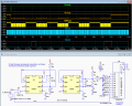
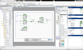
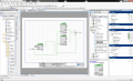
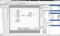
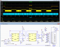
Below is the LTspice simulation of my take on the 555 and CD4017 circuit to do what you want.
The first 555, U3 generates the slow CLK pulse to the CD4017 counter to alternate between the two PWM signals.
U1 generates pulses with a nominal 20ms period (Out, blue trace) that goes to the servo.
U2 causes the pulse width to alternate between a nominal 1ms and 2ms, as it sequences through its 5 pulse sequence (yellow trace) and alternately applys 6V (for1ms) and 0V (for 2ms) to R5.
When Q9 goes high at the last pulse, that Stop signal (brown trace) at the input to NAND gate U4 pulls the 555 Reset input low and stops it from outputting pulses.
To start the sequence, the NAND gate Start input (from an IR sensor input if desired) goes momentarily from 6V to 0V (green trace).
(You can use a spare NAND gate as in inverter if you want the Start signal to go from 0V to 6V instead.)
The first 555, U3 generates the slow CLK pulse to the CD4017 counter to alternate between the two PWM signals.
U1 generates pulses with a nominal 20ms period (Out, blue trace) that goes to the servo.
U2 causes the pulse width to alternate between a nominal 1ms and 2ms, as it sequences through its 5 pulse sequence (yellow trace) and alternately applys 6V (for1ms) and 0V (for 2ms) to R5.
When Q9 goes high at the last pulse, that Stop signal (brown trace) at the input to NAND gate U4 pulls the 555 Reset input low and stops it from outputting pulses.
To start the sequence, the NAND gate Start input (from an IR sensor input if desired) goes momentarily from 6V to 0V (green trace).
(You can use a spare NAND gate as in inverter if you want the Start signal to go from 0V to 6V instead.)