Does anyone have an idea of where I can buy a 36 pins QFN-DIP adapter with 2 exposed bottom pads? The pinout of the IC is attached below. Closest I could find was a 38 PIN QFN-DIP adapter and that is not working.
Why not make one? easy to do and cheap.... I did my own TSSOP 20/30/40 0.5mm/0.65mm pad spacing, 0.3/0.4/0.6 adapters - cost me a couple hours of time and under $25 from a chinese pcb shop...
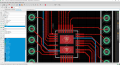
Did not find any pre-made adapters. Took your suggestion and designed my own. The IC is LT3958 and it is a power converter IC that can be used as Boost, Flyback, and SEPIC. I am using it in SEPIC mode to get +15V,-15V, and +5V from a 72V battery pack
Looks good, but I suggest you extend pads 37 & 38 as per datasheet to minimise track inductances. I'd make it a smaller DIP and consolidate pins eg 1,2,4,23, 36,35,34 are all NC and connected to SGND so don't need to be brought out to individual DIP-pins, similarly for SW (38), 8, 9, 10, 20, 21 and the GND pins 12 - 17... , but may need a couple of pins depending on current to/from external components...
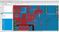
Looking at the SEPIC circuit you actually only need to bring out nominally 8 pins from the carrier, Vin (27), SGND, RT(33) , SS (32), VC (30), FBX (31), GND, SW - I'd put the Vcc bypass capacitor on the carrier from pin 28 to SGND and extend SGND and SW on the back of the carrier to provide additional heatsinking
Looks good, but I suggest you extend pads 37 & 38 as per datasheet to minimise track inductances. I'd make it a smaller DIP and consolidate pins eg 1,2,4,23, 36,35,34 are all NC and connected to SGND so don't need to be brought out to individual DIP-pins, similarly for SW (38), 8, 9, 10, 20, 21 and the GND pins 12 - 17... , but may need a couple of pins depending on current to/from external components...
Looking at the SEPIC circuit you actually only need to bring out nominally 8 pins from the carrier, Vin (27), SGND, RT(33) , SS (32), VC (30), FBX (31), GND, SW - I'd put the Vcc bypass capacitor on the carrier from pin 28 to SGND and extend SGND and SW on the back of the carrier to provide additional heatsinking
Left it that way because it will be easier to orient and solder the IC onto the board. I don't have any hot air guns or Reflow machines and need to do them by hand for the prototypes at least. So having those pins separate will help with alignment.
Does anyone have an idea of where I can buy a 36 pins QFN-DIP adapter with 2 exposed bottom pads? The pinout of the IC is attached below. Closest I could find was a 38 PIN QFN-DIP adapter and that is not working.
You're welcome. It's not perfect, I still don't like the long runs. Try turning the QFN 45 or 90degrees anticlockwise so the individual pins end up on both sides at top and SW and GND end up on opposite sides at bottom..
You're welcome. It's not perfect, I still don't like the long runs. Try turning the QFN 45 or 90degrees anticlockwise so the individual pins end up on both sides at top and SW and GND end up on opposite sides at bottom..
Yeah. Will do something like this (pic attached below). The screenshot is from my complete design of the final product. Wanted to test it on a breadboard before sending it for PCB manufacturing and ran into this trouble
Hmm, why not just make up a small test pcb with just the buck converter on it to verify the layout? You could make a board with a few candidate layouts so you can compare and contrast them. That's what I would do rather than mess with a dip carrier which may introduce other side effects...
Hmm, why not just make up a small test pcb with just the buck converter on it to verify the layout? You could make a board with a few candidate layouts so you can compare and contrast them. That's what I would do rather than mess with a dip carrier which may introduce other side effects...
And you can't swap parts on a PCB? Breadboarding an SMPS rarely gets the results you expect, too many stray inductances/capacitances and lack of ground planes - modern SMPS chips are quite finicky in this respect. Also lead lengths of through-hole passives on a bb don't translate well to SMD parts on a PCB.
In your position I would make a few small test PCBs, using larger SMD parts so easy to hand-solder so I could do proper evaluation of the PSU or other circuit characteristics if I wasn't confident enough about the design before releasing to manufacturing - especially if its going on a multilayer board. In one example I had something like 15 'modules' each on their own mini-board., which were then stuck down on a wooden baseboard. That allowed me to test relative positions/distances/screening/etc between the subsystems and identified where we might have had issues on the final assembly. Simply being able to rotate one particular module 90 degrees identified and removed a massive interference/crosstalk problem that would have been a real issue if it hadn't been caught at that stage.
 Facebook
 Google
 GitHub
 Linkedin