27C256DC-12 duplication and Atmel 80C32 fault finding

ericgibbs

Joined Jan 29, 2010
21,532
Hi Geoff,
If you are absolutely sure the MCU is faulty.?
I usually cut the legs off, as close to the body of the IC as possible, taking care not to twist as I cut.
It is very important that you do not damage or lift the copper track or the plated through holes.

When the MCU is completely removed, then using fine pointed pliers, heat each of the residual pin pieces one by one and remove. [check that non of the pins are bent over on the underside of the board].
The holes must all be clear of solder, use de-solder wick, I prefer the wick method and if necessary liquid flux.
If you get a problem hole that will not wick clean, a sharpened match stick sometimes helps.

E
 

MrChips

Joined Oct 2, 2009
35,022
Sorry missed your last post!
No once the initial power up happens if you change the dip switches the address doesn't change.

You have to do a power down/up cycle then it will change.
It means that our tests are flawed.
There is no more access to the rotary switch 74HTC573 after the initial power ON. We would have to capture the signals during the power up sequence.
 

Thread Starter

geoffers

Joined Oct 25, 2010
520
Still not 100% sure, but

I know the eprom is ok, the good board runs it.

The 80c32 has a clock input.

The 80c32 has a output on ale.

The watchdog chip isn't receiving a pulse so is repeatedly resetting the 80c32 every 1.6s.

The latch between pins 32-39 and the eprom is not having oe pulled low by the 80c32. Can the latch fail and hold this input high?

I do have some 74hct573's so guess that is easier to change as there not so many pins!

I'll check everything again before I do anything rash!

I'm sure Mr chips will have some more ideas to probe, I guess he's in a different time zone so is probably asleep.

Cheers Geoff
 

Thread Starter

geoffers

Joined Oct 25, 2010
520
No he's not asleep!

I have tested oe(pin1) on the 74hct139 as the board powers and once a 5v it stays there.

Thanks Geoff
 

MrChips

Joined Oct 2, 2009
35,022
Also, you can trigger on the watchdog timer output and watch the signals at the 74HCT573 latch to see if the node address is being read properly.
 

MrChips

Joined Oct 2, 2009
35,022
And even before that happens, trigger on the watchdog timer, check that the 80C32 is receiving the RST signal and it is reading data from the EPROM.
 

Thread Starter

geoffers

Joined Oct 25, 2010
520
Going round the chip

1. H
2. H
3. H
4. H
5. H
6. H (wdt)
7. L buffer oe
8. H
9. High pulse every 1.6s from wdt
10. H
11. H
12. H
13. L. Buffer oe
14. H
15. H
16. H
17. H
18. Clock signal
19. Clock signal
20. L
21. L
22. Reset pulse (same as anyway?)
23. Reset pulse
24. Reset pulse
25. Reset pulse
26. Reset pulse
27. Reset pulse
28. Reset pulse
29. Same as ALE
30. Ale around 60khz
31. L
32. Stream of pulses same as ALE, then a break @ 1.6s (matches reset pulse
33. As 32
34 As 33
35. 12khz pulses, mainly high with a small low pulse, interrupted by reset
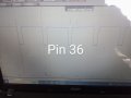
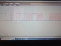
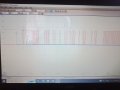
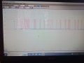
36. 12khz pulse picture below
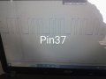
37. Something a bit like data picture below
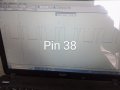
38. As 37
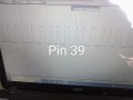
39. As 38
40.
IMG_20230310_134247_330~2.jpg
IMG_20230310_133848_413~2.jpgIMG_20230310_134557_605~2.jpgIMG_20230310_134444_526~2.jpgAll the ones pictured repeat then are interpreted every 1.6s by the reset I assume?

Cheers Geoff
 

MrChips

Joined Oct 2, 2009
35,022
I don't know the capabilities of your pico oscilloscope. What we are looking for is what exactly happens on the address and data bus immediately following the RST signal, or at least the first 1 to 3 instruction cycles.

This will allow us to check for faults in the 80C32 processor, 74HCT138 or 74HCT139 address decoders, 74HCT573 address latch and 27C256 EPROM.

In order to do this we need to set up the picoscope to capture and hold on the RST trigger.
In an ideal world we would be using a digital logic analyzer but that costs more than an arm and a leg. Without that, we have to make do with what we have.

Let me know if the picoscope is capable of capturing a one-shot event. In the meantime, I will try to find the picoscope user manual.

I know that this is asking a lot from you and your test equipment. If this is important to you I don't see too many options.
If we persevere we might get some answers yet.
 

Thread Starter

geoffers

Joined Oct 25, 2010
520
I can set it to trigger on the rising or falling edge of the reset pulse.

It saves around 32 'pages' of signals.
If I've understood it right , trigger on channel a (reset) while reading the data bus with channel b?

Should be able to do that. One time for each pin 32-39?

Thanks again Geoff
 

MrChips

Joined Oct 2, 2009
35,022
Let me give you a synopsis of what to expect and what we are looking for.


1678467098375.png

8051 80C32 pinout.jpg
The processor is reset when RST goes high. It does not matter if we trigger on the rising or falling edge. Since nothing should happen while RST is HIGH it would make sense to trigger on the falling edge of RST.

After a short delay, the MCU (80C32 microcontroller unit) has to begin executing instructions from address $0000 from the 27C256 EPROM.

In order to read the EPROM, the MCU has to send out address $0000 on pins 28-21 (high order byte) and pins 32-39 (low order byte). The low order byte has to be latched into a 74HCT573 on the trailing edge of ALE.

The /CE pin of the EPROM has to receive a decoded signal from one or more address bits from A15-A8 via a 74HCT138 or 74HCT139 or some digital gates. (In this case, since the EPROM is a 32K-byte memory, we would expect that only A15 needs to go to /CE of the EPROM).

The /OE pin of the EPROM has to receive /RD from the MCU and the EPROM's 8-bit data is placed on the AD7-AD0 bus.

What should we be seeing?
We should see the first address on A15-A8 and AD7-AD0 all LOW for the first T1-T2 cycles.
We should see ALE and /RD pulses in their correct timing positions, see drawing below.

At T2-T3 we should see /RD going LOW and the AD7-AD0 bus should change (to some unknown 8-bit value).

On the next T1-T2 cycles, the address should change to $0001.
Again, we should see /RD going LOW and the AD7-AD0 bus should change again to some unknown value.

If we can see these then we have some indication that the MCU, address decoder, address latch, and EPROM are doing something.

1678467987893.png
 

Thread Starter

geoffers

Joined Oct 25, 2010
520
IMG_20230310_173548_367.jpgIMG_20230310_173610_017.jpgIMG_20230310_173631_212.jpgIMG_20230310_173654_136.jpgIMG_20230310_173716_962.jpgIMG_20230310_173744_232.jpgIMG_20230310_173804_329.jpgIMG_20230310_173836_741.jpgIMG_20230310_173903_842.jpgIMG_20230310_173930_237.jpg
Thanks , here is what I scoped, took longer to upload than do the readings
Looks like the 0's come out ok and everything is nice until you look at the rd pin which just stays high.

Cheers Geoff
 

Thread Starter

geoffers

Joined Oct 25, 2010
520
If I haven't quite got the right readings, I hadn't seen your synopsis before I did them! Very informative, thank you
 

MrChips

Joined Oct 2, 2009
35,022
Ok. Thanks.
/RD pin-17 staying HIGH is problematic. Let us focus on pin-17.
Let's not put any blame on the MCU just yet.

/RD pin-17 has to go to a number of places.
Let's see if we can identify where pin-17 goes, by following the PCB tracks and also using the ohmmeter in continuity mode.

I will compile a list of where I think pin-17 needs to go.
With a bit of luck we might find a chip whose input is stuck high.
 

MrChips

Joined Oct 2, 2009
35,022
There is not a lot of additional digital ICs on the board.
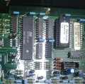
I can see the 80C32, SN74HCT139N, 74HC151N and the EPROM.
Can you identify the four that are hard to read?

80C32 PCB digital ICs.jpg
 

Thread Starter

geoffers

Joined Oct 25, 2010
520
To the left of the 80c32 is a 74hct04

To it's top right two 74hct573

To the eproms bottom left 74hct00e?

As well as the 74hct573 for the node address,

There are two more for motor drive outputs I think?

I've been scraping pins with the multi meter and can only find pin 17 is connected to pin 1 of the 74hct139
 

MrChips

Joined Oct 2, 2009
35,022
Do you know if this is a double sided or multi-layered PCB?
If the tracks on the bottom side are clearly visible can you post a photo of that area of the underside of the PCB?
 
Top