Its probably caused by shoot through where both top and bottom of the H bridge is on at the same time. You need to insert some dead time where both upper and lower halves of the H Bridge are off
it may be what you would expect -- if you assume.. (= your inverter is designed for) ..a "heavy load" by default
- so your smoothing inductor/filter is a relatively low impedance one
options :
design additional filter
(if your modulation is otherwise PWM) make it PFM near low voltage phases --or-- increase your PWM frequency at lower Vout
make multiple switching stages that "share the load" -- enable faster/smoother switching near zero crossing -- basically you insert the lesser amount of energy to output more frequently
etc. ...
From a simulation point of view you could try to put a clock with short on period on the SD line of the H bridge driver such that during the Zero Crossing period the drivers are off, you will need adjust the phase of the pulse so it occurs during the crossover period. In real life you have to do something similar or find an H bridge driver with integrated dead time. I'm pretty sure previously when i helped you on this you were also considering IR2184, if you look at the datasheet there is a IR21844 that has a programmable dead time integrated into it by the look of it. Spend some time looking at the data sheet it may solve your problem
1k pullup for the "339" @ 12V results in apx. 12mA the chip is likely fastest with 4...5mA IC
... the simulation shows a lot less IC with 27kΩ optimal even up/down delay of 190ns for the unloaded "339" output /!\
/!\ only the transition HL starts and completes 190ns earlier than the transition LH so there is ≤ 190ns overlap (both complementary outputs low for that time)
... for 1k pullup the overlap is about the same only the transition HL takes some 580ns
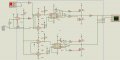
you use 2 comparators - but you basically need only one - at least for the function the LM339 has at your schematic
so you could use simple digital RS (<- Push RESET to clean up the poor simulator). . . or whatever you may find suitable
(silly me) or Vs.total 10V https://www.analog.com/media/en/technical-documentation/data-sheets/1394f.pdf (complementary output thingy)
+
for the synchronous complementary input drive for the half-bridge you just need to select the mosfet with a faster OFF transition than it's ON transition all below switched on at 0ns and off at 200ns
L1+LOAD sees ±32V should be ~ 22.6VRMS Max. . . . but it depends "a little" how you drive the bridge shoulders - for example - if your frequency is too high for the L1 -- it will "eat off" your LOAD power
. . . your drive wave-forms were somewhat confusing for near the 0V drive (if you keep 1 shoulder constantly ON and modulate another such causes the skip to Hi/Lo rails near 0V outp . . . may be partially causing the messy output wave-form there ...)
if C3 R8 is your load , then it - C3 - further draws down the "on the LOAD" dissipation at high frequency drive
? have you simulated/tested it with any success already
 Facebook
 Google
 GitHub
 Linkedin
")